DK-DEV-2AGX260N Altera, DK-DEV-2AGX260N Datasheet - Page 48
DK-DEV-2AGX260N
Manufacturer Part Number
DK-DEV-2AGX260N
Description
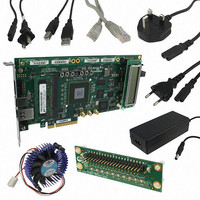
KIT DEV FPGA 2AGX260 W/6.375G TX
Manufacturer
Altera
Series
Arria II GXr
Type
FPGAr
Specifications of DK-DEV-2AGX260N
Contents
Board, Cables, CD, DVD, Power Supply
Silicon Manufacturer
Altera
Core Architecture
FPGA
Core Sub-architecture
Arria
Silicon Core Number
EP2
Silicon Family Name
Arria II GX
Rohs Compliant
Yes
For Use With/related Products
EP2AGX260
Lead Free Status / RoHS Status
Lead free / RoHS Compliant
Other names
544-2696
Available stocks
Company
Part Number
Manufacturer
Quantity
Price
Company:

Part Number:
DK-DEV-2AGX260N
Manufacturer:
Altera
Quantity:
135


2–40
Table 2–39. DDR3 Pin Assignments, Schematic Signal Names, and Functions (Part 2 of 2)
Table 2–40. DDR3 Component Reference and Manufacturing Information
DDR2 SODIMM
Arria II GX FPGA Development Board, 6G Edition Reference Manual
Board Reference
Board Reference
U13.H3
U13.H8
U13.G2
U13.H7
U13.G3
U13.D7
U13.D3
U13.E3
U13.E7
U13.C3
U13.C8
U13.C2
U13.A7
U13.A2
U13.B8
U13.A3
U13.C7
U13.B7
U13.F7
U13.F2
U13.F8
U13.F3
U13
8 M × 16 × 8 banks, 667M, CL9 Micron
Data bus byte lane 0
Data bus byte lane 0
Data bus byte lane 0
Data bus byte lane 0
Data bus byte lane 0
Data bus byte lane 0
Data bus byte lane 0
Data bus byte lane 0
Write mask byte lane 0
Data strobe P byte lane 0
Data strobe N byte lane 0
Data bus byte lane 1
Data bus byte lane 1
Data bus byte lane 1
Data bus byte lane 1
Data bus byte lane 1
Data bus byte lane 1
Data bus byte lane 1
Data bus byte lane 1
Write mask byte lane 1
Data strobe P byte lane 1
Data strobe N byte lane 1
Table 2–40
There is a DDR2 200-pin SODIMM device, providing 1-Gbyte single-rank DIMM with
a 64-bit data bus. This memory interface is designed to run at a maximum fequency of
333 MHz for a maximum theoretical bandwidth of over 42.6 Gbps. The internal bus in
the FPGA is typically 2 or 4 times the width at full rate or half rate respectively. For
example, a 333 MHz 64-bit interface will become a 166.5 MHz 256-bit bus.
Table 2–41
The signal names and types are relative to the Arria II device in terms of I/O setting
and direction.
Description
Description
lists the DDR3 component reference and manufacturing information.
lists the DDR2 SODIMM pin assignments, signal names, and its functions.
DDR3_DQ0
DDR3_DQ1
DDR3_DQ2
DDR3_DQ3
DDR3_DQ4
DDR3_DQ5
DDR3_DQ6
DDR3_DQ7
DDR3_DM0
DDR3_DQS_P0
DDR3_DQS_N0
DDR3_DQ8
DDR3_DQ9
DDR3_DQ10
DDR3_DQ11
DDR3_DQ12
DDR3_DQ13
DDR3_DQ14
DDR3_DQ15
DDR3_DM1
DDR3_DQS_P1
DDR3_DQS_N1
Manufacturer
Schematic Signal
Name
MT41J64M16LA-15E
Manufacturing
Part Number
1.5-V SSTL Class I
I/O Standard
© July 2010 Altera Corporation
Chapter 2: Board Components
www.micron.com
Manufacturer
Website
Pin Number
Arria II GX
Device
G14
D13
D12
G15
G13
K17
L16
K15
E12
J16
F15
F13
J15
F12
B7
A6
A3
A4
B3
B9
A2
B4
Memory
Related parts for DK-DEV-2AGX260N
Image
Part Number
Description
Manufacturer
Datasheet
Request
R

Part Number:
Description:
KIT DEV ARRIA II GX FPGA 2AGX125
Manufacturer:
Altera
Datasheet:

Part Number:
Description:
KIT DEV CYCLONE III LS EP3CLS200
Manufacturer:
Altera
Datasheet:

Part Number:
Description:
KIT DEV STRATIX IV FPGA 4SE530
Manufacturer:
Altera
Datasheet:

Part Number:
Description:
KIT DEV MAX V 5M570Z
Manufacturer:
Altera
Datasheet:

Part Number:
Description:
KIT DEV STRATIX V FPGA 5SGXEA7
Manufacturer:
Altera
Datasheet:

Part Number:
Description:
KIT DEVELOPMENT STRATIX III
Manufacturer:
Altera
Datasheet:

Part Number:
Description:
KIT DEVELOPMENT STRATIX IV
Manufacturer:
Altera
Datasheet:

Part Number:
Description:
KIT DEV ARRIA GX 1AGX60N
Manufacturer:
Altera
Datasheet:
Part Number:
Description:
KIT STARTER CYCLONE IV GX
Manufacturer:
Altera
Datasheet:
Part Number:
Description:
KIT DEVELOPMENT STRATIX IV
Manufacturer:
Altera
Datasheet:

Part Number:
Description:
CPLD, EP610 Family, ECMOS Process, 300 Gates, 16 Macro Cells, 16 Reg., 16 User I/Os, 5V Supply, 35 Speed Grade, 24DIP
Manufacturer:
Altera Corporation
Datasheet:
Part Number:
Description:
CPLD, EP610 Family, ECMOS Process, 300 Gates, 16 Macro Cells, 16 Reg., 16 User I/Os, 5V Supply, 15 Speed Grade, 24DIP
Manufacturer:
Altera Corporation
Datasheet: