DK-DEV-2AGX260N Altera, DK-DEV-2AGX260N Datasheet - Page 39
DK-DEV-2AGX260N
Manufacturer Part Number
DK-DEV-2AGX260N
Description
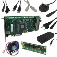
KIT DEV FPGA 2AGX260 W/6.375G TX
Manufacturer
Altera
Series
Arria II GXr
Type
FPGAr
Specifications of DK-DEV-2AGX260N
Contents
Board, Cables, CD, DVD, Power Supply
Silicon Manufacturer
Altera
Core Architecture
FPGA
Core Sub-architecture
Arria
Silicon Core Number
EP2
Silicon Family Name
Arria II GX
Rohs Compliant
Yes
For Use With/related Products
EP2AGX260
Lead Free Status / RoHS Status
Lead free / RoHS Compliant
Other names
544-2696
Available stocks
Company
Part Number
Manufacturer
Quantity
Price
Company:

Part Number:
DK-DEV-2AGX260N
Manufacturer:
Altera
Quantity:
135


Chapter 2: Board Components
Components and Interfaces
Table 2–35. Ethernet PHY Component Reference and Manufacturing Information
High-Speed Mezzanine Cards
© July 2010 Altera Corporation
Board Reference
U24
f
Ethernet PHY BASE-T device
Table 2–35
information.
The development board contains two HSMC interfaces called port A and port B. The
HSMC port B is only available in the Arria II GX FPGA development board, 6G
Edition. HSMC port A interface supports both single-ended and differential signaling
while HSMC port B interface only supports single-ended signaling. The HSMC
interface also allows JTAG, SMB, clock outputs and inputs, as well as power for
compatible HSMC cards. The HSMC is an Altera-developed open specification, which
allows you to expand the functionality of the development board through the
addition of daughtercards (HSMCs).
For more information about the HSMC specification such as signaling standards,
signal integrity, compatible connectors, and mechanical information, refer to the
Speed Mezzanine Card (HSMC) Specification
The HSMC connector has a total of 172 pins, including 120 signal pins, 39 power pins,
and 13 ground pins. The ground pins are located between the two rows of signal and
power pins, acting both as a shield and a reference. The HSMC host connector is
based on the 0.5 mm-pitch QSH/QTH family of high-speed, board-to-board
connectors from Samtec. There are three banks in this connector. Bank 1 has every
third pin removed as done in the QSH-DP/QTH-DP series. Bank 2 and bank 3 have
all the pins populated as done in the QSH/QTH series.
Figure 2–10
connector's three banks.
Figure 2–10. HSMC Signal and Bank Diagram
Description
lists the Ethernet PHY interface component reference and manufacturing
shows the bank arrangement of signals with respect to the Samtec
Marvell
Semiconductor
Manufacturer
8 RX Channels CDR
8 TX Channels CDR
CLKIN2, CLKOUT2
CLKIN1, CLKOUT1
CLKIN0, CLKOUT0
Arria II GX FPGA Development Board, 6G Edition Reference Manual
D[3:0] + LVDS
D(79.40)
D(39:0)
Bank 2
Bank 3
Bank 1
Power
Power
LVDS
manual.
JTAG
SMB
88E1111-B2-CAAIC000
-or-
-or-
Manufacturing
Part Number
www.marvell.com
Manufacturer
Website
High
2–31
Related parts for DK-DEV-2AGX260N
Image
Part Number
Description
Manufacturer
Datasheet
Request
R

Part Number:
Description:
KIT DEV ARRIA II GX FPGA 2AGX125
Manufacturer:
Altera
Datasheet:

Part Number:
Description:
KIT DEV CYCLONE III LS EP3CLS200
Manufacturer:
Altera
Datasheet:

Part Number:
Description:
KIT DEV STRATIX IV FPGA 4SE530
Manufacturer:
Altera
Datasheet:

Part Number:
Description:
KIT DEV MAX V 5M570Z
Manufacturer:
Altera
Datasheet:

Part Number:
Description:
KIT DEV STRATIX V FPGA 5SGXEA7
Manufacturer:
Altera
Datasheet:

Part Number:
Description:
KIT DEVELOPMENT STRATIX III
Manufacturer:
Altera
Datasheet:

Part Number:
Description:
KIT DEVELOPMENT STRATIX IV
Manufacturer:
Altera
Datasheet:

Part Number:
Description:
KIT DEV ARRIA GX 1AGX60N
Manufacturer:
Altera
Datasheet:
Part Number:
Description:
KIT STARTER CYCLONE IV GX
Manufacturer:
Altera
Datasheet:
Part Number:
Description:
KIT DEVELOPMENT STRATIX IV
Manufacturer:
Altera
Datasheet:

Part Number:
Description:
CPLD, EP610 Family, ECMOS Process, 300 Gates, 16 Macro Cells, 16 Reg., 16 User I/Os, 5V Supply, 35 Speed Grade, 24DIP
Manufacturer:
Altera Corporation
Datasheet:
Part Number:
Description:
CPLD, EP610 Family, ECMOS Process, 300 Gates, 16 Macro Cells, 16 Reg., 16 User I/Os, 5V Supply, 15 Speed Grade, 24DIP
Manufacturer:
Altera Corporation
Datasheet: