DK-DEV-2AGX260N Altera, DK-DEV-2AGX260N Datasheet - Page 21
DK-DEV-2AGX260N
Manufacturer Part Number
DK-DEV-2AGX260N
Description
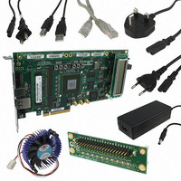
KIT DEV FPGA 2AGX260 W/6.375G TX
Manufacturer
Altera
Series
Arria II GXr
Type
FPGAr
Specifications of DK-DEV-2AGX260N
Contents
Board, Cables, CD, DVD, Power Supply
Silicon Manufacturer
Altera
Core Architecture
FPGA
Core Sub-architecture
Arria
Silicon Core Number
EP2
Silicon Family Name
Arria II GX
Rohs Compliant
Yes
For Use With/related Products
EP2AGX260
Lead Free Status / RoHS Status
Lead free / RoHS Compliant
Other names
544-2696
Available stocks
Company
Part Number
Manufacturer
Quantity
Price
Company:

Part Number:
DK-DEV-2AGX260N
Manufacturer:
Altera
Quantity:
135


Chapter 2: Board Components
Configuration, Status, and Setup Elements
© July 2010 Altera Corporation
f
The default method is to use the factory design called the Board Update Portal. This
design is an embedded webserver, which serves the Board Update Portal web page.
The web page allows you to select new FPGA designs including hardware, software,
or both in an industry-standard S-Record File (.flash) and write the design to the user
hardware page (page 1) of the flash memory over the network.
The secondary method is to use the pre-built parallel flash loader (PFL) design
included in the development kit. The development board implements the Altera PFL
megafunction for flash memory programming. The PFL megafunction is a block of
logic that is programmed into an Altera programmable logic device (FPGA or CPLD).
The PFL functions as a utility for writing to a compatible flash memory device. This
pre-built design contains the PFL megafunction that allows you to write either page 0,
page 1, or other areas of flash memory over the USB interface using the Quartus II
software. This method is used to restore the development board to its factory default
settings.
Other methods to program the flash memory can be used as well, including the
Nios
For more information on the Nios II processor, refer to the
the Altera website.
FPGA Programming from Flash Memory
On either power-up or by pressing the load image push-button switch (PB5), the
MAX II CPLD EPM2210 System Controller's PFL configures the FPGA from the flash
memory when the CONFIG_LED0 is ON. The PFL megafunction reads 16-bit data
from the flash memory and converts it to fast passive parallel (FPP) format. This 8-bit
data is then written to the FPGA's dedicated configuration pins during configuration.
®
II processor.
Arria II GX FPGA Development Board, 6G Edition Reference Manual
Nios II Processor
page of
2–13
Related parts for DK-DEV-2AGX260N
Image
Part Number
Description
Manufacturer
Datasheet
Request
R

Part Number:
Description:
KIT DEV ARRIA II GX FPGA 2AGX125
Manufacturer:
Altera
Datasheet:

Part Number:
Description:
KIT DEV CYCLONE III LS EP3CLS200
Manufacturer:
Altera
Datasheet:

Part Number:
Description:
KIT DEV STRATIX IV FPGA 4SE530
Manufacturer:
Altera
Datasheet:

Part Number:
Description:
KIT DEV MAX V 5M570Z
Manufacturer:
Altera
Datasheet:

Part Number:
Description:
KIT DEV STRATIX V FPGA 5SGXEA7
Manufacturer:
Altera
Datasheet:

Part Number:
Description:
KIT DEVELOPMENT STRATIX III
Manufacturer:
Altera
Datasheet:

Part Number:
Description:
KIT DEVELOPMENT STRATIX IV
Manufacturer:
Altera
Datasheet:

Part Number:
Description:
KIT DEV ARRIA GX 1AGX60N
Manufacturer:
Altera
Datasheet:
Part Number:
Description:
KIT STARTER CYCLONE IV GX
Manufacturer:
Altera
Datasheet:
Part Number:
Description:
KIT DEVELOPMENT STRATIX IV
Manufacturer:
Altera
Datasheet:

Part Number:
Description:
CPLD, EP610 Family, ECMOS Process, 300 Gates, 16 Macro Cells, 16 Reg., 16 User I/Os, 5V Supply, 35 Speed Grade, 24DIP
Manufacturer:
Altera Corporation
Datasheet:
Part Number:
Description:
CPLD, EP610 Family, ECMOS Process, 300 Gates, 16 Macro Cells, 16 Reg., 16 User I/Os, 5V Supply, 15 Speed Grade, 24DIP
Manufacturer:
Altera Corporation
Datasheet: