DK-DEV-2AGX260N Altera, DK-DEV-2AGX260N Datasheet - Page 11
DK-DEV-2AGX260N
Manufacturer Part Number
DK-DEV-2AGX260N
Description
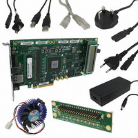
KIT DEV FPGA 2AGX260 W/6.375G TX
Manufacturer
Altera
Series
Arria II GXr
Type
FPGAr
Specifications of DK-DEV-2AGX260N
Contents
Board, Cables, CD, DVD, Power Supply
Silicon Manufacturer
Altera
Core Architecture
FPGA
Core Sub-architecture
Arria
Silicon Core Number
EP2
Silicon Family Name
Arria II GX
Rohs Compliant
Yes
For Use With/related Products
EP2AGX260
Lead Free Status / RoHS Status
Lead free / RoHS Compliant
Other names
544-2696
Available stocks
Company
Part Number
Manufacturer
Quantity
Price
Company:

Part Number:
DK-DEV-2AGX260N
Manufacturer:
Altera
Quantity:
135


Chapter 2: Board Components
Board Overview
Table 2–1. Arria II GX FPGA Development Board, 6G Edition Components (Part 2 of 3)
© July 2010 Altera Corporation
D11, D12, D13
D19, D20, D21,
D22, D23
D4, D5
D6
D2, D3
D1
D24, D25, D26
Clock Circuitry
U26
U30
Y5
Y6
U25
J10, J11
J12
General User Input/Output
D7, D8, D9, D10
SW2
PB3
PB4
PB1, PB2
PB6
PB5
Board Reference
Configuration LEDs
Ethernet LEDs
HSMC port A LEDs
HSMC port A present LED
HSMC port B LEDs
HSMC port B present LED
PCI Express link LEDs
Programmable oscillator
(125 MHz default)
Programmable oscillator
(100 MHz default)
50 MHz oscillator
100 MHz oscillator
155.52 MHz oscillator
Clock input SMAs
Clock output SMA
User LEDs
User DIP switch
CPU reset push-button switch
MAX II reset push-button
switch
General user push-button
switches
Image select push-button
switch
Load image push-button
switch
Type
Illuminates to show the LED sequence that determines which flash
memory image loads to the FPGA when LOAD IMAGE is pressed.
Shows the connection speed as well as transmit or receive activity.
You can configure these LEDs to indicate transmit or receive activity.
Illuminates when a daughtercard is plugged into the HSMC port A.
You can configure these LEDs to indicate transmit or receive activity
(only populated when a EP2AGX260 device is installed).
Illuminates when a daughtercard is plugged into the HSMC port B
(only populated when a EP2AGX260 device is installed).
You can configure these LEDs to display the PCI Express link width
(x1, x4, x8).
Programmable oscillator with a default frequency of 125.00 MHz. The
frequency is programmable using the MAX II CPLD EPM2210 System
Controller. For general use such as memories, gigabit Ethernet
(125 M/156.25 M), Serial RapidIO™ (SRIO) (125 M), or PCI Express
(100 M).
Programmable oscillator with a default frequency of 100.00 MHz. The
frequency is programmable using the MAX II CPLD EPM2210 System
Controller. For general use such as memories, gigabit Ethernet
(125 M/156.25 M), SRIO (125 M), PCI Express (100 M), or XAUI
(156.25 M). Multiplex with CLKIN_SMA_P based on CLK_SEL
switch value.
50.000 MHz crystal oscillator for general purpose logic.
100.000 MHz crystal oscillator for general purpose logic.
155.520 MHz crystal oscillator for SONET.
Drive LVPECL-compatible clock inputs into the clock multiplexer buffer
(U33).
Drive out 2.5-V CMOS clock output from the FPGA.
Four user LEDs. Illuminates when driven low.
Quad user DIP switches. When the switch is ON, a logic 0 is selected.
Press to reset the FPGA logic.
Press to reset the MAX II CPLD EPM2210 System Controller.
Two user push-button switches. Driven low when pressed.
Toggles the configuration LEDs which selects the program image that
loads from flash memory to the FPGA.
Load image from flash memory to the FGPA based on the
configuration LED setting.
Arria II GX FPGA Development Board, 6G Edition Reference Manual
Description
2–3
Related parts for DK-DEV-2AGX260N
Image
Part Number
Description
Manufacturer
Datasheet
Request
R

Part Number:
Description:
KIT DEV ARRIA II GX FPGA 2AGX125
Manufacturer:
Altera
Datasheet:

Part Number:
Description:
KIT DEV CYCLONE III LS EP3CLS200
Manufacturer:
Altera
Datasheet:

Part Number:
Description:
KIT DEV STRATIX IV FPGA 4SE530
Manufacturer:
Altera
Datasheet:

Part Number:
Description:
KIT DEV MAX V 5M570Z
Manufacturer:
Altera
Datasheet:

Part Number:
Description:
KIT DEV STRATIX V FPGA 5SGXEA7
Manufacturer:
Altera
Datasheet:

Part Number:
Description:
KIT DEVELOPMENT STRATIX III
Manufacturer:
Altera
Datasheet:

Part Number:
Description:
KIT DEVELOPMENT STRATIX IV
Manufacturer:
Altera
Datasheet:

Part Number:
Description:
KIT DEV ARRIA GX 1AGX60N
Manufacturer:
Altera
Datasheet:
Part Number:
Description:
KIT STARTER CYCLONE IV GX
Manufacturer:
Altera
Datasheet:
Part Number:
Description:
KIT DEVELOPMENT STRATIX IV
Manufacturer:
Altera
Datasheet:

Part Number:
Description:
CPLD, EP610 Family, ECMOS Process, 300 Gates, 16 Macro Cells, 16 Reg., 16 User I/Os, 5V Supply, 35 Speed Grade, 24DIP
Manufacturer:
Altera Corporation
Datasheet:
Part Number:
Description:
CPLD, EP610 Family, ECMOS Process, 300 Gates, 16 Macro Cells, 16 Reg., 16 User I/Os, 5V Supply, 15 Speed Grade, 24DIP
Manufacturer:
Altera Corporation
Datasheet: