MCIMX35WPDKJ Freescale Semiconductor, MCIMX35WPDKJ Datasheet - Page 48
MCIMX35WPDKJ
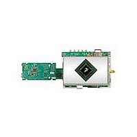
Manufacturer Part Number
MCIMX35WPDKJ
Description
BOARD DEV FOR I.MX35
Manufacturer
Freescale Semiconductor
Series
i.MX35r
Type
MPUr
Datasheets
1.MCIMX35WPDKJ.pdf
(148 pages)
2.MCIMX35WPDKJ.pdf
(2 pages)
3.MCIMX35WPDKJ.pdf
(10 pages)
Specifications of MCIMX35WPDKJ
Contents
Module and Misc Hardware
Processor To Be Evaluated
i.MX35
Processor Series
i.MX35
Data Bus Width
32 bit
Interface Type
RS-232, Ethernet, USB, CAN, JTAG
Core
ARM11
For Use With/related Products
i.MX35
Lead Free Status / RoHS Status
Lead free / RoHS Compliant


48
SD1
SD2
SD3
SD6
ID
ADDR
RAS
CAS
SDCLK
SDCLK
WE
CS
SDRAM clock high-level width
SDRAM clock low-level width
SDRAM clock cycle time
Address setup time
SD6
Test conditions are: pin voltage 1.7 V–1.95 V, capacitance 15 pF for all pins
(both DDR and non-DDR pins), drive strength is high (7.2 mA). “High” is
defined as 80% of signal value and “low” is defined as 20% of signal value.
SDR SDRAM CLK parameters are measured from the 50% point—that is,
“high” is defined as 50% of signal value, and “low” is defined as 50% of
signal value. tCH + tCL will not exceed 7.5 ns for 133 MHz. DDR SDRAM
CLK parameters are measured at the crossing point of SDCLK and SDCLK
(inverted clock).
The timing parameters are similar to the ones used in SDRAM data sheets.
Table 34
the ESDCTL at the negative edge of SDCLK, and the parameters are
measured at maximum memory frequency.
i.MX35 Applications Processors for Industrial and Consumer Products, Rev. 9
BA
indicates SDRAM requirements. All output signals are driven by
SD7
Table 35. SDRAM Refresh Timing Parameters
Figure 29. SDRAM Refresh Timing Diagram
SD11
Parameter
NOTE
SD10
SD1
SD3
Symbol
tCH
tCK
tCL
tAS
SD2
SD10
Min.
3.4
3.4
7.5
1.8
ROW/BA
Freescale Semiconductor
Max.
4.1
4.1
—
—
Unit
ns
ns
ns
ns
Related parts for MCIMX35WPDKJ
Image
Part Number
Description
Manufacturer
Datasheet
Request
R

Part Number:
Description:
MCIMX-LVDS1
Manufacturer:
Freescale Semiconductor
Datasheet:

Part Number:
Description:
Manufacturer:
Freescale Semiconductor, Inc
Datasheet:
Part Number:
Description:
Manufacturer:
Freescale Semiconductor, Inc
Datasheet:
Part Number:
Description:
Manufacturer:
Freescale Semiconductor, Inc
Datasheet:
Part Number:
Description:
Manufacturer:
Freescale Semiconductor, Inc
Datasheet:
Part Number:
Description:
Manufacturer:
Freescale Semiconductor, Inc
Datasheet:
Part Number:
Description:
Manufacturer:
Freescale Semiconductor, Inc
Datasheet:
Part Number:
Description:
Manufacturer:
Freescale Semiconductor, Inc
Datasheet:
Part Number:
Description:
Manufacturer:
Freescale Semiconductor, Inc
Datasheet:
Part Number:
Description:
Manufacturer:
Freescale Semiconductor, Inc
Datasheet:
Part Number:
Description:
Manufacturer:
Freescale Semiconductor, Inc
Datasheet:
Part Number:
Description:
Manufacturer:
Freescale Semiconductor, Inc
Datasheet:
Part Number:
Description:
Manufacturer:
Freescale Semiconductor, Inc
Datasheet:
Part Number:
Description:
Manufacturer:
Freescale Semiconductor, Inc
Datasheet:
Part Number:
Description:
Manufacturer:
Freescale Semiconductor, Inc
Datasheet: