DM163035 Microchip Technology, DM163035 Datasheet - Page 82
DM163035
Manufacturer Part Number
DM163035
Description
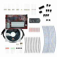
KIT DEVELOPMENT PICDEM LAB
Manufacturer
Microchip Technology
Type
MCUr
Datasheet
1.DM163035.pdf
(96 pages)
Specifications of DM163035
Contents
Board, Cable, Components, CD, PICkit Programmer
Processor To Be Evaluated
PIC10F, PIC12F615, PIC16F616
Data Bus Width
8 bit
Operating Supply Voltage
1.3 V to 5 V
Silicon Manufacturer
Microchip
Core Architecture
PIC
Core Sub-architecture
PIC10, PIC12, PIC16
Silicon Core Number
PIC10F, PIC12F, PIC16F
Silicon Family Name
PIC10F2xx, PIC12F6xx, PIC16F6xx
Lead Free Status / RoHS Status
Lead free / RoHS Compliant
For Use With/related Products
PIC10F206, PIC16F690, PIC16F819
Lead Free Status / Rohs Status
Lead free / RoHS Compliant


PICDEM
DS41369A-page 78
TM
The Initialize() configures the peripherals as follows:
• Ports
• ADC
Next, the Get_Inputs() performs an ADC on the voltage present on pin 13. The
internal capacitor connected to the input of the ADC peripheral needs time to charge to
the voltage present on the pin. Therefore, software will need to implement a short delay
to allow for this charging time. The ADC Module section “A/D Acquisition Require-
ments” of the data sheet goes into great detail and includes an equation for selecting
an appropriate acquisition time. For the purposes of this lab, a simple 1mS delay
should be more than sufficient. These parameters become important in high-speed
applications where every μS counts.
The GO/DONE bit in ADCON0 is used to start the ADC process when set to ‘1’. This
bit also serves as a flag that indicates when the ADC is completed (GO/DONE = 0).
Therefore, the Get_Inputs() initiates an ADC by setting GO/DONE then sits and
waits for the bit to clear indicating a completed conversion.
The software flowchart for the Get_Inputs() is shown in Figure 5-3.
Lab Development Board User’s Guide
- Configure pin 13 as an analog input (using TRISB4).
- Clear the PORTC register.
- Configure RC0, RC1, RC2 and RC3 pins as digital output.
- Select ADC conversion clock F
- Configure voltage reference using V
- Select channel 10 as the ADC input channel (Pin 13: RB4/AN10).
- Select result format left justified (10-bit result in ADRESH<7:0> and
- Turn on ADC module.
Note:
ADRESL<7:6>).
The ADC conversion clock is the time that will be used to convert the analog
voltage present on pin 13 to a 10-bit value in the ADRESH:ADRESL regis-
ters. It takes 11 of these conversion clock cycles to perform a complete
ADC. If the conversion clock period is insufficient, an incomplete ADC result
will occur. The electrical specifications for the PIC16F690 state that the
conversion clock must have a period of at least 1.5
quency of approximately 667 kHz. The ADC Module section of the data
sheet specifies acceptable conversion clock frequencies depending on the
main oscillator used to drive the microcontroller and should be referenced.
In this application, a dedicated internal oscillator for the ADC module is
used ensuring a conversion clock frequency of between 2-6
(see Table 17-16 in Section 17 of the PIC16F690 Data Sheet).
RC .
DD
.
© 2009 Microchip Technology Inc.
μ
Seconds or a fre-
μ
Seconds.
Related parts for DM163035
Image
Part Number
Description
Manufacturer
Datasheet
Request
R

Part Number:
Description:
Manufacturer:
Microchip Technology Inc.
Datasheet:
Part Number:
Description:
Manufacturer:
Microchip Technology Inc.
Datasheet:
Part Number:
Description:
Manufacturer:
Microchip Technology Inc.
Datasheet:
Part Number:
Description:
Manufacturer:
Microchip Technology Inc.
Datasheet:
Part Number:
Description:
Manufacturer:
Microchip Technology Inc.
Datasheet:
Part Number:
Description:
Manufacturer:
Microchip Technology Inc.
Datasheet:
Part Number:
Description:
Manufacturer:
Microchip Technology Inc.
Datasheet:
Part Number:
Description:
Manufacturer:
Microchip Technology Inc.
Datasheet: