DM163035 Microchip Technology, DM163035 Datasheet - Page 37
DM163035
Manufacturer Part Number
DM163035
Description
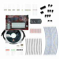
KIT DEVELOPMENT PICDEM LAB
Manufacturer
Microchip Technology
Type
MCUr
Datasheet
1.DM163035.pdf
(96 pages)
Specifications of DM163035
Contents
Board, Cable, Components, CD, PICkit Programmer
Processor To Be Evaluated
PIC10F, PIC12F615, PIC16F616
Data Bus Width
8 bit
Operating Supply Voltage
1.3 V to 5 V
Silicon Manufacturer
Microchip
Core Architecture
PIC
Core Sub-architecture
PIC10, PIC12, PIC16
Silicon Core Number
PIC10F, PIC12F, PIC16F
Silicon Family Name
PIC10F2xx, PIC12F6xx, PIC16F6xx
Lead Free Status / RoHS Status
Lead free / RoHS Compliant
For Use With/related Products
PIC10F206, PIC16F690, PIC16F819
Lead Free Status / Rohs Status
Lead free / RoHS Compliant


© 2009 Microchip Technology Inc.
EXAMPLE 3-9:
3. Finally, copy/paste the code in Example 3-10 into the Timing() over the code
EXAMPLE 3-10:
4. The remaining code from the previous lab remains the same. Compile the proj-
3.3.6.4
Program the PIC16F690. The application should behave exactly as it did in the
previous lab. Using an oscilloscope to test individual PORTC pin level transitions would
be useful to analyze the accuracy of the delay.
The solution for this project is located in the
C:\PICDEM_Lab\GPIO_Labs\GPIO_Lab3\solution directory.
Note:
//Set all PORTC bits HIGH (to a known state)
from the previous lab
ect. There should be no errors.
PORTC = 0b11111111;
//Configure PORTC's ANALOG/DIGITAL pins as all Digital
ANS4 = 0;//Associated with RC0
ANS5 = 0;//Associated with RC1
ANS6 = 0;//Associated with RC2
ANS7 = 0;//Associated with RC3
ANS8 = 0;//Associated with RC6
ANS9 = 0;//Associated with RC7
//Configure PORTC pins as all output
//i.e. 1 = Input, 0 = Output
TRISC0 = 0;//Make RC0 (pin 16) output
TRISC1 = 0;//Make RC1 (pin 15) output
TRISC2 = 0;//Make RC2 (pin 14) output
TRISC3 = 0;//Make RC3 (pin 7) output
TRISC4 = 0;//Make RC4 (pin 6) output
TRISC5 = 0;//Make RC5 (pin 5) output
TRISC6 = 0;//Make RC6 (pin 8) output
TRISC7 = 0;//Make RC7 (pin 9) output
//Configure Timer0 as follows:
T0CS = 0; //Use the internal instruction clock
T0SE = 0;//Increment TMR0 on low-to-high
PSA = 0;//Assign the prescaler to
//Configure Timer0 prescaler to increment
//TMR0 every 256 FOSC/4 clock transitions
PS0 = 1;
PS1 = 1;
PS2 = 1;
Delay_1S(); //Call the 1 second delay
TESTING THE APPLICATION
More in-depth tutorials on the Timer0 peripheral are covered in “Timers:
Timer0 Tutorial (Part 1)” (5162a.pdf) and “Timers: Timer0 Tutorial (Part 2)”
(51702a.pdf) files included on the PICDEM™ Lab Development Kit CD.
General Purpose Input/Output Labs
//FOSC/4 as the clock source
//FOSC/4 transition
//Timer0
INITIALIZE() CODE FOR LAB 3
TIMING() CODE FOR LAB 3
DS41369A-page 33
Related parts for DM163035
Image
Part Number
Description
Manufacturer
Datasheet
Request
R

Part Number:
Description:
Manufacturer:
Microchip Technology Inc.
Datasheet:
Part Number:
Description:
Manufacturer:
Microchip Technology Inc.
Datasheet:
Part Number:
Description:
Manufacturer:
Microchip Technology Inc.
Datasheet:
Part Number:
Description:
Manufacturer:
Microchip Technology Inc.
Datasheet:
Part Number:
Description:
Manufacturer:
Microchip Technology Inc.
Datasheet:
Part Number:
Description:
Manufacturer:
Microchip Technology Inc.
Datasheet:
Part Number:
Description:
Manufacturer:
Microchip Technology Inc.
Datasheet:
Part Number:
Description:
Manufacturer:
Microchip Technology Inc.
Datasheet: