DK-DEV-3CLS200N Altera, DK-DEV-3CLS200N Datasheet - Page 21
DK-DEV-3CLS200N
Manufacturer Part Number
DK-DEV-3CLS200N
Description
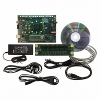
KIT DEV CYCLONE III LS EP3CLS200
Manufacturer
Altera
Series
Cyclone® IIIr
Type
FPGAr
Datasheets
1.EP3C5F256C8N.pdf
(34 pages)
2.EP3C5F256C8N.pdf
(14 pages)
3.DK-START-3C25N.pdf
(74 pages)
4.DK-DEV-3CLS200N.pdf
(42 pages)
Specifications of DK-DEV-3CLS200N
Contents
Board
Silicon Manufacturer
Altera
Core Architecture
FPGA
Core Sub-architecture
Cyclone
Silicon Core Number
EP3C
Silicon Family Name
Cyclone III LS
Rohs Compliant
Yes
For Use With/related Products
EP3CLS200
Lead Free Status / RoHS Status
Lead free / RoHS Compliant
Other names
544-2601


Chapter 6: Board Test System
Preparing the Board
Preparing the Board
Running the Board Test System
Using the Board Test System
© October 2009 Altera Corporation
1
1
c
With the power to the board off, perform the following steps:
1. Connect the USB cable to the board.
2. Verify the settings for the board settings DIP switch bank (SW2) match
3. Set the PGM/USER LOAD switch (SW2.6) to the off position.
4. Verify the settings for the JTAG jumper blocks (J11 and J12) match
5. Turn the power to the board on. The board loads the design stored in the user
To ensure operating stability, keep the USB cable connected and the board powered on
when running the demonstration application. The application cannot run correctly
unless the USB cable is attached and the board is on.
To run the application, navigate to the <install
dir>\kits\cycloneIIILS_3cls200_fpga\examples\board_test_system directory and
run the BoardTestSystem.exe application.
On Windows, click Start > All Programs > Altera > Cyclone III LS FPGA
Development Kit <version> > Board Test System to run the application.
A GUI appears, displaying the application tab that corresponds to the design running
in the FPGA. The Cyclone III LS FPGA development board’s flash memory ships
preconfigured with the design that corresponds to the Config, GPIO, and
SRAM&Flash tabs.
If you power up your board with the PGM/USER LOAD switch (SW2.6) in the on
position, or if you load your own design into the FPGA with the Quartus II
Programmer, you receive a message prompting you to configure your board with a
valid Board Test System design. Refer to
configuring your board.
This section describes each control in the Board Test System application.
on page
page
f
portion of flash memory into the FPGA. If your board is still in the factory
configuration or if you have downloaded a newer version of the Board Test
System to flash memory through the Board Update Portal, the design that tests the
GPIO, SRAM, and flash memory loads.
4–3. These settings determine the devices to include in the JTAG chain.
For more information about the board’s DIP switch and jumper settings,
refer to the
4–2.
Cyclone III LS FPGA Development Board Reference
“The Configure Menu”
Cyclone III LS FPGA Development Kit User Guide
for information about
Table 4–3 on
Manual.
Table 4–2
6–3
Related parts for DK-DEV-3CLS200N
Image
Part Number
Description
Manufacturer
Datasheet
Request
R

Part Number:
Description:
KIT DEV ARRIA II GX FPGA 2AGX125
Manufacturer:
Altera
Datasheet:

Part Number:
Description:
KIT DEV STRATIX IV FPGA 4SE530
Manufacturer:
Altera
Datasheet:

Part Number:
Description:
KIT DEV FPGA 2AGX260 W/6.375G TX
Manufacturer:
Altera
Datasheet:

Part Number:
Description:
KIT DEV MAX V 5M570Z
Manufacturer:
Altera
Datasheet:

Part Number:
Description:
KIT DEV STRATIX V FPGA 5SGXEA7
Manufacturer:
Altera
Datasheet:

Part Number:
Description:
KIT DEVELOPMENT STRATIX III
Manufacturer:
Altera
Datasheet:

Part Number:
Description:
KIT DEVELOPMENT STRATIX IV
Manufacturer:
Altera
Datasheet:

Part Number:
Description:
KIT DEV ARRIA GX 1AGX60N
Manufacturer:
Altera
Datasheet:
Part Number:
Description:
KIT STARTER CYCLONE IV GX
Manufacturer:
Altera
Datasheet:
Part Number:
Description:
KIT DEVELOPMENT STRATIX IV
Manufacturer:
Altera
Datasheet:

Part Number:
Description:
CPLD, EP610 Family, ECMOS Process, 300 Gates, 16 Macro Cells, 16 Reg., 16 User I/Os, 5V Supply, 35 Speed Grade, 24DIP
Manufacturer:
Altera Corporation
Datasheet:
Part Number:
Description:
CPLD, EP610 Family, ECMOS Process, 300 Gates, 16 Macro Cells, 16 Reg., 16 User I/Os, 5V Supply, 15 Speed Grade, 24DIP
Manufacturer:
Altera Corporation
Datasheet: