DK-DEV-3CLS200N Altera, DK-DEV-3CLS200N Datasheet - Page 13
DK-DEV-3CLS200N
Manufacturer Part Number
DK-DEV-3CLS200N
Description
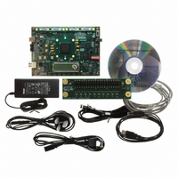
KIT DEV CYCLONE III LS EP3CLS200
Manufacturer
Altera
Series
Cyclone® IIIr
Type
FPGAr
Datasheets
1.EP3C5F256C8N.pdf
(34 pages)
2.EP3C5F256C8N.pdf
(14 pages)
3.DK-START-3C25N.pdf
(74 pages)
4.DK-DEV-3CLS200N.pdf
(42 pages)
Specifications of DK-DEV-3CLS200N
Contents
Board
Silicon Manufacturer
Altera
Core Architecture
FPGA
Core Sub-architecture
Cyclone
Silicon Core Number
EP3C
Silicon Family Name
Cyclone III LS
Rohs Compliant
Yes
For Use With/related Products
EP3CLS200
Lead Free Status / RoHS Status
Lead free / RoHS Compliant
Other names
544-2601


Introduction
Setting Up the Board
© October 2009 Altera Corporation
f
1
The instructions in this chapter explain how to set up the Cyclone III LS FPGA
development board.
To set up and power up the board, perform the following steps:
1. The Cyclone III LS FPGA development board ships with its board switches
2. The development board ships with example designs stored in the flash memory
3. Connect the DC adapter (+16 V, 3.75 A) to the DC power jack (J5) on the FPGA
4. Set the POWER switch (SW1) to the on position. When power is supplied to the
The MAX II device on the board contains a parallel flash loader (PFL) megafunction.
When the board powers up, the PFL reads one of two designs from flash memory and
configures the FPGA. The PGM/USER LOAD switch (SW2.6) controls which design
to load. When the switch is in the on position, the PFL loads the design from the
factory portion of flash memory. When the switch is in the off position, the PFL loads
the design from the user portion of flash memory.
The development kit includes the MAX II configuration design in the <install
dir>\kits\cycloneIIILS_3cls200_fpga\examples\max2 directory.
When configuration is complete, the CONF DONE LED (D14) illuminates, signaling
that the Cyclone III LS device configured successfully. If the loaded design has the
Quartus II software INIT_DONE option on, the FPGA INIT DONE LED (D14)
illuminates when the device enters user mode.
For more information about the PFL megafunction, refer to
Flash Loader with the Quartus II
preconfigured to support the example designs in the development kit. If you
suspect your board might not be currently configured with the default settings,
follow the instructions in
the board to its factory settings before proceeding.
device. Verify the PGM/USER LOAD switch (SW2.6) is set to the on position to
load the design stored in the factory portion of flash memory.
switch location on the Cyclone III LS FPGA development board.
board and plug the cord into a power outlet.
c
board, a blue LED (D3) illuminates indicating that the board has power.
Use only the supplied power supply. Power regulation circuitry on the
board can be damaged by power supplies with greater voltage.
“Factory Default Switch Settings” on page 4–2
Software.
4. Development Board Setup
Cyclone III LS FPGA Development Kit User Guide
AN 386: Using the Parallel
Figure 4–1
shows the
to return
Related parts for DK-DEV-3CLS200N
Image
Part Number
Description
Manufacturer
Datasheet
Request
R

Part Number:
Description:
KIT DEV ARRIA II GX FPGA 2AGX125
Manufacturer:
Altera
Datasheet:

Part Number:
Description:
KIT DEV STRATIX IV FPGA 4SE530
Manufacturer:
Altera
Datasheet:

Part Number:
Description:
KIT DEV FPGA 2AGX260 W/6.375G TX
Manufacturer:
Altera
Datasheet:

Part Number:
Description:
KIT DEV MAX V 5M570Z
Manufacturer:
Altera
Datasheet:

Part Number:
Description:
KIT DEV STRATIX V FPGA 5SGXEA7
Manufacturer:
Altera
Datasheet:

Part Number:
Description:
KIT DEVELOPMENT STRATIX III
Manufacturer:
Altera
Datasheet:

Part Number:
Description:
KIT DEVELOPMENT STRATIX IV
Manufacturer:
Altera
Datasheet:

Part Number:
Description:
KIT DEV ARRIA GX 1AGX60N
Manufacturer:
Altera
Datasheet:
Part Number:
Description:
KIT STARTER CYCLONE IV GX
Manufacturer:
Altera
Datasheet:
Part Number:
Description:
KIT DEVELOPMENT STRATIX IV
Manufacturer:
Altera
Datasheet:

Part Number:
Description:
CPLD, EP610 Family, ECMOS Process, 300 Gates, 16 Macro Cells, 16 Reg., 16 User I/Os, 5V Supply, 35 Speed Grade, 24DIP
Manufacturer:
Altera Corporation
Datasheet:
Part Number:
Description:
CPLD, EP610 Family, ECMOS Process, 300 Gates, 16 Macro Cells, 16 Reg., 16 User I/Os, 5V Supply, 15 Speed Grade, 24DIP
Manufacturer:
Altera Corporation
Datasheet: