MPC8313E-RDB Freescale Semiconductor, MPC8313E-RDB Datasheet - Page 96
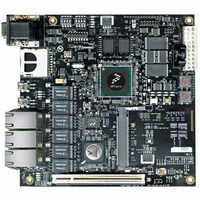
MPC8313E-RDB
Manufacturer Part Number
MPC8313E-RDB
Description
BOARD PROCESSOR
Manufacturer
Freescale Semiconductor
Series
PowerQUICC II™ PROr
Type
MCUr
Datasheets
1.MPC8313CZQAFFB.pdf
(100 pages)
2.MPC8313E-RDBB.pdf
(52 pages)
3.MPC8313E-RDBB.pdf
(2 pages)
Specifications of MPC8313E-RDB
Contents
Reference Design Board, Software and Documentation
Termination Type
SMD
Supply Voltage Max
1.05V
Tool / Board Applications
Wired Connectivity-LIN, CAN, Ethernet, USB
Mcu Supported Families
POWERQUICC II PRO
Rohs Compliant
Yes
Filter Terminals
SMD
Silicon Manufacturer
Freescale
Silicon Core Number
MPC83xx
Kit Application Type
Communication & Networking
Application Sub Type
Ethernet
Core Architecture
Power Architecture
Silicon Family Name
PowerQUICC II PRO
For Use With/related Products
MPC8313E
Lead Free Status / RoHS Status
Lead free / RoHS Compliant


Document Revision History
96
Number
Rev.
1
0
3/2008
6/2007
Date
MPC8313E PowerQUICC
Initial release.
• In Table 63, added LBC_PM_REF_10 & LSRCID3 as muxed with USBDR_PCTL1
• In Table 63, added LSRCID2 as muxed with USBDR_PCTL0
• In Table 63, added LSRCID1 as muxed with USBDR_PWRFAULT
• In Table 63, added LSRCID0 as muxed with USBDR_DRIVE_VBUS
• In Table 63, moved T1, U2,& V2 from V
• In Table 63, moved P2, R2, & T3 from V
• In Table 63, moved P5, & U4 from V
• In Table 63, moved P3, & V4 from V
• In Table 63, removed “Double with pad” for AV
• In Table 63, added impedance control requirements for SD_IMP_CAL_TX (100 ohms to GND) and
• In Table 63, updated muxing in pinout to show new options for selecting IEEE 1588 functionality.
• In Table 63, updated muxing in pinout to show new LBC ECC boot enable control muxed with
• Added pin type information for power supplies.
• Removed N1 and N3 from Vss section of Table 63. Added Therm0 and Therm1 (N1 and N3,
• In Table 65 corrected maximum frequency of Local Bus Frequency from “33–66” to 66 MHz
• In Table 65 corrected maximum frequency of PCI from “24–66” to 66 MHz
• Added “which is determined by RCWLR[COREPLL],” to the note in Section 20.2, “Core PLL
• Added “(VCOD)” next to VCO divider column in Table 68. Added footnote stating that core_clk
• In Table 69, notes were confusing. Added note 3 for VCO column, note 4 for CSB ( csb_clk ) column,
• In Table 69, updated note 6 to specify USB reference clock frequencies limited to 24 and 48 for rev.
• Replaced Table 71 “Thermal Resistance for TEPBGAII with Heat Sink in Open Flow”.
• Removed last row of Table 19.
• Removed 200 MHz rows from Table 21 and Table 5.
• Changed VIH minimum spec from 2.0 to 2.1 for clock, PIC, JTAG, SPI, and reset pins in Table 9,
• Added Figure 4 showing the DDR input timing diagram.
•
• Added “and power” to rows 2 and 3 in Table 10
• Added the sentence “Once both the power supplies...” and PORESET to Section 2.2, “Power
• In Figure 35, corrected “USB0_CLK/USB1_CLK/DR_CLK” with “USBDR_CLK”
• In Table 42, clarified that AC specs are for ULPI only.
and Ground Supplies section
SD_IMP_CAL_RX (200 ohms to GND).
Added footnote 8
eTSEC1_MDC
respectively). Added note 7 to state: “Internal thermally sensitive resistor, resistor value varies
linearly with temperature. Useful for determining the junction temperature.”
Configuration” about the VCO divider.
frequency must not exceed its maximum, so 2.5:1 and 3:1 core_clk:csb_clk ratios are invalid for
certain csb_clk values.
note 5 for USB ref column, and note 6 to replace “Note 1”. Clarified note 4 to explain erratum
eTSEC40.
2 silicon.
Table 47, Table 54, Table 59, and Table 61.
In Table 19, removed “MDM” from the “M
column for the tCISKEW parameter. MDM is an output signal and should be removed from
the input AC timing spec table (tCISKEW).
Sequencing,” and Figure 3.
Table 73. Document Revision History (continued)
™
II Pro Processor Hardware Specifications, Rev. 3
SS
Substantive Change(s)
DD
to XPADVSS.
DD
to XPADVDD.
SS
DQS-MDQ/MECC/MDM” text under the Parameter
to XCOREVDD.
to XCOREVSS.
DD1
and AV
DD2
and moved AV
Freescale Semiconductor
DD1
and AV
DD2
to Power
Related parts for MPC8313E-RDB
Image
Part Number
Description
Manufacturer
Datasheet
Request
R

Part Number:
Description:
Mpc8313e Powerquicc Ii Pro Processor
Manufacturer:
Freescale Semiconductor, Inc
Datasheet:

Part Number:
Description:
BOARD CPU 8313E VER 2.1
Manufacturer:
Freescale Semiconductor
Datasheet:

Part Number:
Description:
BOARD CPU 8313E VER 2.2
Manufacturer:
Freescale Semiconductor
Datasheet:
Part Number:
Description:
Microprocessors - MPU 8313 REV2.2 PB ENC EXT
Manufacturer:
Freescale Semiconductor
Datasheet:
Part Number:
Description:
Microprocessors - MPU 8313 REV2.2 PB W/ENC
Manufacturer:
Freescale Semiconductor
Datasheet:
Part Number:
Description:
Microprocessors - MPU 8313 REV2.2 PB NO EN EXT
Manufacturer:
Freescale Semiconductor
Datasheet:
Part Number:
Description:
Microprocessors - MPU 8313 REV2.2 PB NO ENC
Manufacturer:
Freescale Semiconductor
Datasheet:
Part Number:
Description:
Manufacturer:
Freescale Semiconductor, Inc
Datasheet:
Part Number:
Description:
Manufacturer:
Freescale Semiconductor, Inc
Datasheet:
Part Number:
Description:
Manufacturer:
Freescale Semiconductor, Inc
Datasheet:
Part Number:
Description:
Manufacturer:
Freescale Semiconductor, Inc
Datasheet:
Part Number:
Description:
Manufacturer:
Freescale Semiconductor, Inc
Datasheet:
Part Number:
Description:
Manufacturer:
Freescale Semiconductor, Inc
Datasheet:
Part Number:
Description:
Manufacturer:
Freescale Semiconductor, Inc
Datasheet:
Part Number:
Description:
Manufacturer:
Freescale Semiconductor, Inc
Datasheet: