MPC8313E-RDB Freescale Semiconductor, MPC8313E-RDB Datasheet
MPC8313E-RDB
Specifications of MPC8313E-RDB


Related parts for MPC8313E-RDB


MPC8313E-RDB Summary of contents
Page 1
... Board-Level Functions . . . . . . . . . . . . . . . . . . . . . . . . 7 3. Connectors, Jumpers, Switches, and LEDs . . . . . . . 19 4. Micro-Jumper/Resistor Options for eTSEC1 . . . . . . 27 5. MPC8313E RDB Board Configuration . . . . . . . . . . 38 6. Getting Started . . . . . . . . . . . . . . . . . . . . . . . . . . . . . 43 7. MPC8313E RDB Software . . . . . . . . . . . . . . . . . . . . 46 8. Frequently Asked Questions (FAQs Revision History . . . . . . . . . . . . . . . . . . . . . . . . . . . . 49 WARNING This is a class A product domestic environment this product may cause radio interference, in which case the user may be required to take adequate measures ...
Page 2
... MPC8313E RDB Hardware This section covers the features, block diagram, specifications, and mechanical data of the MPC8313E RDB. 1.1 Features The board features are as follows: • ...
Page 3
... IEEE Std. 1588™ signals for test and measurement • Real-time clock and thermal sensor on I • Programmable LEDs for debug use • 6-layer PCB routing (4-layer signals, 2-layer power and ground) PowerQUICC™ MPC8313E Reference Design Board (RDB), Rev. 4 Freescale Semiconductor 2 C bus MPC8313E RDB Hardware 3 ...
Page 4
... Flash Memory LEDs/status Buffers Real-Time Thermal EEPROM Clock Sensor LCD Connectors JTAG/COP Header Power Supply with Low Power Mode PowerQUICC™ MPC8313E Reference Design Board (RDB), Rev MPC8313E 33/66 MHz eTSEC1 PCI Bus 32-Bit DDR2 Bus 16-Bit Local Bus eTSEC2 On-Chip USB 2 I ...
Page 5
... Storage temperature Relative humidity PCB dimensions: Length Width Thickness PowerQUICC™ MPC8313E Reference Design Board (RDB), Rev. 4 Freescale Semiconductor Table 1. MPC8313E-RDB Specifications Typical Maximum 5.0 V DC1 mA1.5 A MPC8313E running at 266 MHz 4 Gbyte (32 address lines) 8 Mbyte with one chip-select 128 Mbyte DDR2 SDRAM ...
Page 6
... Mechanical Data Figure 2 shows the MPC8313E RDB REVAx and REVB dimensions (in mil and [mm]). The board measures 170 mm × 170 mm (6693 mil × 6693 mil) for integration in a mini-ITX chassis. Figure 2. Dimensions of the MPC8313E RDB (REVAx and REVB) PowerQUICC™ MPC8313E Reference Design Board (RDB), Rev. 4 ...
Page 7
... Figure 3 shows the MPC8313E RDB Rev C dimensions (in mil and [mm]). The board measures 195 mm × 170 mm (7692 mil × 6693 mil). Figure 3. Dimensions of the MPC8313E RDB (REVC) 2 Board-Level Functions The board-level functions are reset, external interrupts, clock distribution, DDR SDRAM controller, local ...
Page 8
... Board-Level Functions 2.1 Reset and Reset Configurations The MPC8313E RDB reset module generates a single reset to the MPC8313E and other peripherals on the board. The reset unit provides power-on reset, hard reset, and soft reset signals in compliance with the MPC8313E hardware specification. Figure 4 shows the reset circuitry. Note the following: • ...
Page 9
... IRQ3 is connected to the L2 switch as well external USB PHY (by an optional resistor). • IRQ4 is connected to the Marvell GBE PHY as well as to RTC and LM75 (by an optional resistors). PowerQUICC™ MPC8313E Reference Design Board (RDB), Rev. 4 Freescale Semiconductor SD Card PCI slot (AD15) INTA Figure 5 ...
Page 10
... PLL GTX_CLK125 local bus 125MHz 125 MHz LVDS SD_REF_CLK OSC IEEE1588 TMR CLK 24 MHz Crystal Real-Time Clock GND GND Figure 6. MPC8313E-RDB Clock Scheme 33/66 MHz 0 NC 33/66 MHz 1 Mini PCI Slot 2 33/66 MHz PCI Slot PCI_SYNC_OUT PCI_SYNC_IN LCLKx (NC) PLL MCK DDR ...
Page 11
... DDR2 devices used. DDR2 supports on-die termination; the T DDR2 chips and MPC8313E are connected directly. The interface is 1.8 V provided by an on-board PowerQUICC™ MPC8313E Reference Design Board (RDB), Rev. 4 Freescale Semiconductor Table 2. Clock Distribution Generated by 66 ...
Page 12
... Board-Level Functions voltage regulator. VREF, which is half the interface voltage provided by a voltage divider of 1.8 V for voltage tracking and low cost. The MPC8313E provides a pair of clock pins, which are connected and shared by the two DDR2 devices. Figure 7 shows the DDR2 SDRAM controller connection. ...
Page 13
... LA[24:16] LAD[15:0] WE0 GPL2 2.5.2 NAND Flash Memory The MPC8313E has native support for NAND Flash memory through its NAND Flash control machine (FCM). The MPC8313E RDB implements an 8-bit NAND Flash with 32 Mbyte in size. the NAND Flash connection. MPC8313E eLBC Controller ...
Page 14
... MPC8313E, as well as to store the configuration registers’ values and user program if the MPC8313E boot sequencer is enabled. By default, the EEPROM is not used and the hard reset configuration words are loaded from local bus flash memory. For details about how to program PowerQUICC™ ...
Page 15
... I2C1-SDA 2.7 SD Memory Card Interface An SD memory card interface connects directly to the SPI bus of the MPC8313E. SD data mode and SDIO mode are not supported. The SPI mode is the only SD operating mode supported by this connection. Hot insertion and removal is not supported. See ...
Page 16
... Local Bus 2.8 USB Interface MPC8313E supports a USB 2.0 high speed host/device interface through its on-chip USB PHY or external ULPI USB PHY. The MPC8313E RDB supports both options. By default, the on-chip USB PHY is used. Figure 13 shows the USB connections. MPC8313E USB-DP ...
Page 17
... Figure 14. RGMII Interface Connection for L2 Switch 2.10 eTSEC2 10/100/1000 BaseT Interface eTESC2 can be set to operate in RGMII mode (default) or SGMII mode. connection for eTSEC. MPC8313E eTSEC2 PowerQUICC™ MPC8313E Reference Design Board (RDB), Rev. 4 Freescale Semiconductor VSC7385 L2 switch RGMII RGMII SGMII 88E1111 ...
Page 18
... PCI Bus The 32-bit PCI interface connects to a 32-bit 3.3 V PCI slot and a miniPCI slot (see MPC8313E 32Bit PCI PCI-AD[0:31] PCI-CBE[0:3] PCI-CTRL PCI-GNT0 PCI-REQ0 PCI-GNT1 PCI-REQ1 PowerQUICC™ MPC8313E Reference Design Board (RDB), Rev Figure 16 illustrates the serial port connection using a MAX3232 ...
Page 19
... Ethernet port, USB port, parallel port, RS-232, and so on. A typical setup using a USB port emulator is shown in Figure 18. PC USB Port Figure 18. Connecting MPC8313E-RDB to a USB Emulator The 16-pin generic header connector carries the COP/JTAG signals and the additional signals for system debugging. The pinout of this connector is shown in 3 Connectors, Jumpers, Switches, and LEDs Table 3 summarizes the connectors, jumpers, switches, and LEDs on the MPC8313E RDB and provides the number of the section/page on which each is discussed ...
Page 20
... MCU programming connector. J24 is used for MCU programming on the RDB reserved. J19 Open (Default)—Power ON controlled by switch; Close—Power is always ON S1 System reset button. Resets the MPC8313E RDB. (PORESET). Press once on the push button reset switch on the RDB to cause a power-on reset (PORESET) to the board. S2 Power ON button. Press once to power ON/OFF. ...
Page 21
... PCI Slot (P2) The MPC8313E RDB has one 32-bit 3.3-V PCI expansion slot (P2) for an expansion card. The slot connects AD15 for its device select signal. Only the 3.3-V PCI card is supported. Turn OFF power during PowerQUICC™ MPC8313E Reference Design Board (RDB), Rev. 4 ...
Page 22
... USB Connectors (P4, P8) There are two USB connectors on the MPC8313E RDB. One connects to the on-chip PHY of the MPC8313E, and the other connects to the external ULPI USB PHY. Either can be enabled at a time. The PowerQUICC™ MPC8313E Reference Design Board (RDB), Rev. 4 ...
Page 23
... PHY USB is used. 3.5 Ethernet Connectors (P5, P6, P7) The MPC8313E RDB has six Ethernet ports (RJ-45). The first five ports (G0–G4) are supported by eTSEC1 (L2 switch), and the last port (G5) is supported by eTSEC2 (GBE PHY). G0–G5 mapping viewing from the front panel. ...
Page 24
... LCD Connectors (J21, J22) Two headers (J21, J22) are provided for LCD connections. They use the MPC8313E GPIO interface. Both headers carry the same set of GPIO signal pins, but they are different physically. J21 is single row of 1 × 14, and J22 is double row of 2 × 7. ...
Page 25
... IEEE 1588 Connector (Optional) A header (P10) is provided for IEEE 1588 signals connection double row of 2 × 8 header connector. The pinout of this connector is shown in (Optional if not used by TSEC1 PHY) TSEC_TMR_GCLK PowerQUICC™ MPC8313E Reference Design Board (RDB), Rev. 4 Freescale Semiconductor Pin Number Description 7 Pull-down ...
Page 26
... DIP switch S3 selects the reset configuration source (RST_CFG_SRC) for the MPC8313E. shows the factory default configuration of S3. Check the MPC8313E reference manual for the meaning of the CFG_RST_SRC combination. By default, the DIP switch is set to all ON, meaning CFG_RST_SRC[0..3] = 0000. In this case, the hardware reset configuration is loaded from local bus NOR flash memory ...
Page 27
... LEDs, and 0xFF turns off all LEDs. 4 Micro-Jumper/Resistor Options for eTSEC1 The eTSEC1 RGMII, ULPI USB, and IEEE 1588 signals are multiplexed on the MPC8313E. The MPC8313E RDB supports switching among the three interfaces using micro-jumpers (REVA boards) or resistor options (REVA1 or later boards). ...
Page 28
... Table 6. Default Micro-jumper Settings for REVA Jumper Setting J13 1-2 J12 1-2 J16 1-2 J15 1-2 J17 1-2 J14 1-2 J11 open J10 1-2 PowerQUICC™ MPC8313E Reference Design Board (RDB), Rev Figure 30. REVA Micro-jumper Locations Table 6. Jumper Setting Jumper Setting ...
Page 29
... Table 8. Alternative Micro-jumper Settings for REVA (Setup 3) Jumper Setting J13 open J12 open J16 open J15 open J17 open J14 2-3 J11 2-3 J10 2-3 PowerQUICC™ MPC8313E Reference Design Board (RDB), Rev. 4 Freescale Semiconductor Table 7. Jumper Setting Jumper Setting J7 2-3 J5 2-3 J9 2-3 J1 2-3 J6 2-3 J2 ...
Page 30
... Because the eTSEC1 Ethernet switch PHY on the RDB supports only RGMII, the eTSEC1 SGMII is not supported. The micro-jumper settings listed only matter for the eTSEC1 pin connections. They have nothing to do with switching between eTSEC2 RGMII and SGMII. The settings of eTSEC2 SGMII are provided as a reference. PowerQUICC™ MPC8313E Reference Design Board (RDB), Rev Table 9. ...
Page 31
... Setting R258 short R259 open R260 short R261 open R262 short R263 open R264 short PowerQUICC™ MPC8313E Reference Design Board (RDB), Rev. 4 Freescale Semiconductor Table 10 shows the default configuration. Resistor Setting Resistor Setting R267 open R276 short R268 short R277 ...
Page 32
... R259 short R260 open R261 short R262 open R263 short R264 open R265 short R266 open PowerQUICC™ MPC8313E Reference Design Board (RDB), Rev Resistor Setting Resistor Setting R274 short R283 open R275 open R284 short Resistor Setting Resistor Setting ...
Page 33
... R259 short R260 open R261 short R262 open R263 short R264 open R265 short R266 open PowerQUICC™ MPC8313E Reference Design Board (RDB), Rev. 4 Freescale Semiconductor Resistor Setting Resistor Setting R267 short R276 open R268 open R277 short R269 short R278 ...
Page 34
... R259 open R260 short R261 open R262 short R263 open R264 short R265 open R266 short PowerQUICC™ MPC8313E Reference Design Board (RDB), Rev Resistor Setting Resistor Setting R267 open R276 short R268 short R277 open R269 open R278 short ...
Page 35
... For REVC boards, 22 more resistor options (R311–R313) are added to route eTSEC2 RGMII signals either to L2 Switch or Marvell 88E1111 PHY. All other resistor options are the same as on the REVB boards. PowerQUICC™ MPC8313E Reference Design Board (RDB), Rev. 4 Freescale Semiconductor ...
Page 36
... R121 short R333 R345 open R334 R122 short R335 Figure 36 shows the graphical representation for Setup 1. Figure 36. Setup 2 Resistor Options for REVC PowerQUICC™ MPC8313E Reference Design Board (RDB), Rev Setting Resistor Setting Resistor open R336 short R370 short R337 open ...
Page 37
... SGMII signals to PHY Table 17. Setup 3 Resistor Options for REVC Resistor Setting Resistor R118 open R346 R342 short R123 PowerQUICC™ MPC8313E Reference Design Board (RDB), Rev. 4 Freescale Semiconductor Setting Resistor Setting Resistor open R336 short R370 short R337 open ...
Page 38
... PCI agent card connected to the miniPCI or PCI slot MHz-only card is inserted, the M66EN signal is driven the PCI agent card according to the PCI specification. However pulled can perform at 66 MHz. By default, the MPC8313E RDB runs its PCI interfaces at 66 MHz unless a 33-MHz PCI card is inserted. ...
Page 39
... Field TSEC1M Figure 40. Reset Configuration Word High (RCWH) Bit Settings Bits Name 0 LBCM 1 DDRCM 2–3 — PowerQUICC™ MPC8313E Reference Design Board (RDB), Rev. 4 Freescale Semiconductor Table 18. Default RCW in Flash Memory Address 62626262 62626262 04040404 00000000 00000000 00000000 A0A0A0A0 A0A0A0A0 60606060 ...
Page 40
... SPMF[0–3] 4–7 SPMF[0–3] 8 — 9–15 COREPLL [0–6] 9–15 COREPLL [0–6] 16–31 — PowerQUICC™ MPC8313E Reference Design Board (RDB), Rev Meaning System PLL 0000 multiplication factor 0001 0010 (Default) 0011 0100 0101 System PLL 0110 multiplication factor 0111-1111 Reserved Must be cleared ...
Page 41
... BMS 6–7 BOOTSEQ 8 SWEN 9–11 ROMLOC 12–13 RLEXT 14-15 Reserved 16-18 TSEC1M PowerQUICC™ MPC8313E Reference Design Board (RDB), Rev. 4 Freescale Semiconductor Meaning PCI host mode 0 1: Default — Must be cleared PCI1 arbiter 0 1: Default — Must be cleared Core disable mode 0: Default ...
Page 42
... MPC8313E power-down mode is supported. A regulator that can be shut down is implemented for this purpose. The MPC8313E does not require the core supply voltage and IO supply voltages to be applied in any particular order. However, during the power ramp up, before the power supplies are stable, there may be an interval when the IO pins are actively driven ...
Page 43
... Getting Started This section describes how to boot the MPC8313E RDB. The on-board flash memory is preloaded with a flash image from the factory. Before powering up the board, verify that all the on-board DIP switches and jumpers are set to the factory defaults according to the settings listed in Settings,” ...
Page 44
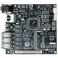
... IEEE 1588 Connector (Optional) Programmable LED0 MPC8313E D20 D22 D21 D4 LCD Backlight LCD Connector J23 D16 J22 D15 D14 D17 J21 D13 LCD Connector Figure 41. MPC8313E-RDB Top View Default Setting S3 0000 (all ON) S4 1111 (all OFF) open (no jumper) Table 23 VBUS D12 CTL0 D10 ...
Page 45
... M-F (upper port for UART1 default; lower port for UART2) 6.3 Serial Port Configuration (PC) Before powering up the MPC8313E RDB, configure the serial port of the attached computer with the following values: • Data rate: 115200 bps • Number of data bits: 8 • ...
Page 46
... The LTIB installation script that installs all necessary packages on <yyyymmdd> a host Linux PC and allows you to modify the BSP and packages within the BSP is in the subdirectory within the ISO image. /ltib-MPC8313E-RDB This ISO image contains a file called MPC8313E RDB hardware platform. ISO image also contains Release Notes ...
Page 47
... BSP on the MPC8313E RDB. This ISO image contains the following documents as well: • . This user's guide document in PDF format. MPC8313ERDBUG.pdf • MPC8313E-RDB_schematic.pdf • . User's guide for the driver software of the security engine. This document details the SEC2SWUG.pdf driver software interface to boost the throughput performance of security applications such as IPSec. ...
Page 48
... Wait for the file transfer and flash programming until you see 7. Power off the board and set DIP switch S3 back to ON-ON-ON-ON (0000). 8. Power on the board and you should see a running u-boot. PowerQUICC™ MPC8313E Reference Design Board (RDB), Rev Table 24. MPC8313E-RBD Revisions ...
Page 49
... Initial public release. 1 4/2007 Replaced a faulty table of contents and restructured sections of the document for clarity. 2 4/2007 Added information to Section 8, Frequently Asked Questions (FAQs) PowerQUICC™ MPC8313E Reference Design Board (RDB), Rev. 4 Freescale Semiconductor Table 25. Document Revision History Substantive Change(s) Revision History 49 ...
Page 50
... Changed default TSEC1_GTX_CLK125 clock source to PLL CY23EP05SX-1 instead of external 125 MHZ oscillator. • Changed U36 1A linear regulator MIC39100-2.5WS to 3A MIC37302WR for higher 2.5V power consumption by additional PHY. • Changed default DAC to 16-bit SPI controlled MAX5203BEUB+ (U47). PowerQUICC™ MPC8313E Reference Design Board (RDB), Rev Substantive Change(s) Freescale Semiconductor ...
Page 51
... THIS PAGE INTENTIONALLY LEFT BLANK PowerQUICC™ MPC8313E Reference Design Board (RDB), Rev. 4 Freescale Semiconductor Revision History 51 ...
Page 52
... Denver, Colorado 80217 +1-800 441-2447 or +1-303-675-2140 Fax: +1-303-675-2150 LDCForFreescaleSemiconductor @hibbertgroup.com Document Number: MPC8313ERDBUG Rev. 4 02/2009 Information in this document is provided solely to enable system and software implementers to use Freescale Semiconductor products. There are no express or implied copyright licenses granted hereunder to design or fabricate any integrated circuits or integrated circuits based on the information in this document ...