MPC8313E-RDB Freescale Semiconductor, MPC8313E-RDB Datasheet - Page 55
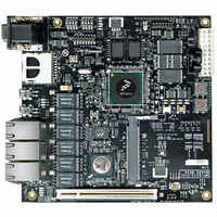
MPC8313E-RDB
Manufacturer Part Number
MPC8313E-RDB
Description
BOARD PROCESSOR
Manufacturer
Freescale Semiconductor
Series
PowerQUICC II™ PROr
Type
MCUr
Datasheets
1.MPC8313CZQAFFB.pdf
(100 pages)
2.MPC8313E-RDBB.pdf
(52 pages)
3.MPC8313E-RDBB.pdf
(2 pages)
Specifications of MPC8313E-RDB
Contents
Reference Design Board, Software and Documentation
Termination Type
SMD
Supply Voltage Max
1.05V
Tool / Board Applications
Wired Connectivity-LIN, CAN, Ethernet, USB
Mcu Supported Families
POWERQUICC II PRO
Rohs Compliant
Yes
Filter Terminals
SMD
Silicon Manufacturer
Freescale
Silicon Core Number
MPC83xx
Kit Application Type
Communication & Networking
Application Sub Type
Ethernet
Core Architecture
Power Architecture
Silicon Family Name
PowerQUICC II PRO
For Use With/related Products
MPC8313E
Lead Free Status / RoHS Status
Lead free / RoHS Compliant


Figure 46
Figure 47
Freescale Semiconductor
All values refer to V
Data hold time:
Fall time of both SDA and SCL signals
Setup time for STOP condition
Bus free time between a STOP and START condition
Noise margin at the LOW level for each connected device (including
hysteresis)
Noise margin at the HIGH level for each connected device (including
hysteresis)
Notes:
1. The symbols used for timing specifications follow the pattern of t
2. The MPC8313E provides a hold time of at least 300 ns for the SDA signal (referred to the V
3. The maximum t
4. C
5. The MPC8313E does not follow the I
inputs and t
with respect to the time data input signals (D) reach the valid state (V) relative to the t
(H) state or setup time. Also, t
(S) went invalid (X) relative to the t
timing (I2) for the time that the data with respect to the stop condition (P) reaching the valid state (V) relative to the t
reference (K) going to the high (H) state or setup time. For rise and fall times, the latter convention is used with the appropriate
letter: R (rise) or F (fall).
the undefined region of the falling edge of SCL.
B
SDA
SCL
= capacitance of one bus line in pF.
provides the AC test load for the I
shows the AC timing diagram for the I
S
(first two letters of functional block)(reference)(state)(signal)(state)
IH
I2DVKH
(min) and V
t
I2CF
t
I2CL
t
MPC8313E PowerQUICC
I2SXKL
has only to be met if the device does not stretch the LOW period (t
Output
Parameter
IL
Table 50. I
(max) levels (see
I2SXKL
I2C
5
symbolizes I
2
clock reference (K) going to the low (L) state or hold time. Also, t
Figure 47. I
C-BUS Specifications, Version 2.1, regarding the t
t
I2DXKL
CBUS compatible masters
2
C AC Electrical Specifications (continued)
Figure 46. I
Table
t
™
I2DVKH
Z
0
II Pro Processor Hardware Specifications, Rev. 3
2
= 50 Ω
t
49).
C timing (I2) for the time that the data with respect to the start condition
I2CH
2
2
I
C.
2
C Bus AC Timing Diagram
C bus devices
t
2
I2SXKL
2
C bus.
C AC Test Load
(first two letters of functional block)(signal)(state)(reference)(state)
for outputs. For example, t
Sr
t
I2SVKH
Symbol
t
t
t
I2PVKH
t
I2KHDX
I2DXKL
R
t
I2KHKL
V
V
I2CF
L
NH
NL
= 50 Ω
1
I2C
0.1 × NV
0.2 × NV
t
clock reference (K) going to the high
I2PVKH
NV
I2CF
Min
I2CL
0.6
1.3
—
0
—
IHmin
I2DVKH
DD
2
t
I2CR
AC parameter.
) of the SCL signal.
/2
DD
DD
of the SCL signal) to bridge
symbolizes I
I2PVKH
P
Max
0.9
300
t
—
—
—
—
—
I2CF
3
symbolizes I
2
C timing (I2)
S
I2C
Unit
μs
ns
μs
μs
clock
for
V
V
2
C
I
55
2
C
Related parts for MPC8313E-RDB
Image
Part Number
Description
Manufacturer
Datasheet
Request
R

Part Number:
Description:
Mpc8313e Powerquicc Ii Pro Processor
Manufacturer:
Freescale Semiconductor, Inc
Datasheet:

Part Number:
Description:
BOARD CPU 8313E VER 2.1
Manufacturer:
Freescale Semiconductor
Datasheet:

Part Number:
Description:
BOARD CPU 8313E VER 2.2
Manufacturer:
Freescale Semiconductor
Datasheet:
Part Number:
Description:
Microprocessors - MPU 8313 REV2.2 PB ENC EXT
Manufacturer:
Freescale Semiconductor
Datasheet:
Part Number:
Description:
Microprocessors - MPU 8313 REV2.2 PB W/ENC
Manufacturer:
Freescale Semiconductor
Datasheet:
Part Number:
Description:
Microprocessors - MPU 8313 REV2.2 PB NO EN EXT
Manufacturer:
Freescale Semiconductor
Datasheet:
Part Number:
Description:
Microprocessors - MPU 8313 REV2.2 PB NO ENC
Manufacturer:
Freescale Semiconductor
Datasheet:
Part Number:
Description:
Manufacturer:
Freescale Semiconductor, Inc
Datasheet:
Part Number:
Description:
Manufacturer:
Freescale Semiconductor, Inc
Datasheet:
Part Number:
Description:
Manufacturer:
Freescale Semiconductor, Inc
Datasheet:
Part Number:
Description:
Manufacturer:
Freescale Semiconductor, Inc
Datasheet:
Part Number:
Description:
Manufacturer:
Freescale Semiconductor, Inc
Datasheet:
Part Number:
Description:
Manufacturer:
Freescale Semiconductor, Inc
Datasheet:
Part Number:
Description:
Manufacturer:
Freescale Semiconductor, Inc
Datasheet:
Part Number:
Description:
Manufacturer:
Freescale Semiconductor, Inc
Datasheet: