MPC8313E-RDB Freescale Semiconductor, MPC8313E-RDB Datasheet - Page 28
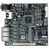
MPC8313E-RDB
Manufacturer Part Number
MPC8313E-RDB
Description
BOARD PROCESSOR
Manufacturer
Freescale Semiconductor
Series
PowerQUICC II™ PROr
Type
MCUr
Datasheets
1.MPC8313CZQAFFB.pdf
(100 pages)
2.MPC8313E-RDBB.pdf
(52 pages)
3.MPC8313E-RDBB.pdf
(2 pages)
Specifications of MPC8313E-RDB
Contents
Reference Design Board, Software and Documentation
Termination Type
SMD
Supply Voltage Max
1.05V
Tool / Board Applications
Wired Connectivity-LIN, CAN, Ethernet, USB
Mcu Supported Families
POWERQUICC II PRO
Rohs Compliant
Yes
Filter Terminals
SMD
Silicon Manufacturer
Freescale
Silicon Core Number
MPC83xx
Kit Application Type
Communication & Networking
Application Sub Type
Ethernet
Core Architecture
Power Architecture
Silicon Family Name
PowerQUICC II PRO
For Use With/related Products
MPC8313E
Lead Free Status / RoHS Status
Lead free / RoHS Compliant


Ethernet: Three-Speed Ethernet, MII Management
8.3
Each SGMII port features a 4-wire AC-coupled serial link from the dedicated SerDes interface of
MPC8313E as shown in
output pin of the SerDes transmitter differential pair features a 50-Ω output impedance. Each input of the
SerDes receiver differential pair features 50-Ω on-die termination to XCOREVSS. The reference circuit
of the SerDes transmitter and receiver is shown in
When an eTSEC port is configured to operate in SGMII mode, the parallel interface’s output signals of
this eTSEC port can be left floating. The input signals should be terminated based on the guidelines
described in
the desired POR configuration requirement on these pins, if applicable.
When operating in SGMII mode, the TSEC_GTX_CLK125 clock is not required for this port. Instead, the
SerDes reference clock is required on SD_REF_CLK and SD_REF_CLK pins.
8.3.1
The characteristics and DC requirements of the separate SerDes reference clock are described in
“High-Speed Serial Interfaces (HSSI).”
8.3.2
Table 31
SD_REF_CLK are not intended to be used with, and should not be clocked by, a spread spectrum clock
source.
8.3.3
Table 32
characteristics. Transmitter DC characteristics are measured at the transmitter outputs (SD_TX[n] and
SD_TX[n]) as depicted in
28
Symbol
t
t
REFCJ
REFPJ
t
REF
lists the SGMII SerDes reference clock AC requirements. Note that SD_REF_CLK and
and
SGMII Interface Electrical Characteristics
REFCLK cycle time
REFCLK cycle-to-cycle jitter. Difference in the period of any two
adjacent REFCLK cycles
Phase jitter. Deviation in edge location with respect to mean
edge location
DC Requirements for SGMII SD_REF_CLK and SD_REF_CLK
AC Requirements for SGMII
SGMII Transmitter and Receiver DC Electrical Characteristics
Section 22.5, “Connection Recommendations,”
Table 33
MPC8313E PowerQUICC
Table 31. SD_REF_CLK and SD_REF_CLK AC Requirements
describe the SGMII SerDes transmitter and receiver AC-coupled DC electrical
Figure
Figure
Parameter Description
15, where C
16.
™
II Pro Processor Hardware Specifications, Rev. 3
TX
is the external (on board) AC-coupled capacitor. Each
Figure
SD_REF_CLK and
33.
as long as such termination does not violate
Min
–50
—
—
SD_REF_CLK
Typ
—
—
8
Freescale Semiconductor
Max
100
50
—
Section 9,
Unit
ns
ps
ps
Related parts for MPC8313E-RDB
Image
Part Number
Description
Manufacturer
Datasheet
Request
R

Part Number:
Description:
Mpc8313e Powerquicc Ii Pro Processor
Manufacturer:
Freescale Semiconductor, Inc
Datasheet:

Part Number:
Description:
BOARD CPU 8313E VER 2.1
Manufacturer:
Freescale Semiconductor
Datasheet:

Part Number:
Description:
BOARD CPU 8313E VER 2.2
Manufacturer:
Freescale Semiconductor
Datasheet:
Part Number:
Description:
Microprocessors - MPU 8313 REV2.2 PB ENC EXT
Manufacturer:
Freescale Semiconductor
Datasheet:
Part Number:
Description:
Microprocessors - MPU 8313 REV2.2 PB W/ENC
Manufacturer:
Freescale Semiconductor
Datasheet:
Part Number:
Description:
Microprocessors - MPU 8313 REV2.2 PB NO EN EXT
Manufacturer:
Freescale Semiconductor
Datasheet:
Part Number:
Description:
Microprocessors - MPU 8313 REV2.2 PB NO ENC
Manufacturer:
Freescale Semiconductor
Datasheet:
Part Number:
Description:
Manufacturer:
Freescale Semiconductor, Inc
Datasheet:
Part Number:
Description:
Manufacturer:
Freescale Semiconductor, Inc
Datasheet:
Part Number:
Description:
Manufacturer:
Freescale Semiconductor, Inc
Datasheet:
Part Number:
Description:
Manufacturer:
Freescale Semiconductor, Inc
Datasheet:
Part Number:
Description:
Manufacturer:
Freescale Semiconductor, Inc
Datasheet:
Part Number:
Description:
Manufacturer:
Freescale Semiconductor, Inc
Datasheet:
Part Number:
Description:
Manufacturer:
Freescale Semiconductor, Inc
Datasheet:
Part Number:
Description:
Manufacturer:
Freescale Semiconductor, Inc
Datasheet: