CYII5SC1300-EVAL Cypress Semiconductor Corp, CYII5SC1300-EVAL Datasheet - Page 8
CYII5SC1300-EVAL
Manufacturer Part Number
CYII5SC1300-EVAL
Description
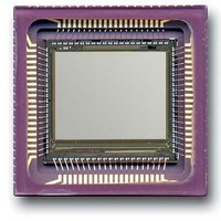
BOARD EVAL IMG SENS IBIS5-B-1300
Manufacturer
Cypress Semiconductor Corp
Specifications of CYII5SC1300-EVAL
Sensor Type
CMOS Imaging, Color (RGB)
Sensing Range
1.3 Megapixel
Interface
Parallel/Serial
Sensitivity
106 fps
Voltage - Supply
3 V ~ 4.5 V
Embedded
No
Utilized Ic / Part
IBIS5-B-1300
Lead Free Status / RoHS Status
Contains lead / RoHS non-compliant
Lead Free Status / RoHS Status
Lead free / RoHS Compliant, Contains lead / RoHS non-compliant


Document #: 38-05710 Rev. *A
The internal resistor R
7.88 k Ω .
The recommend resistor values for both DAC_VLOW and
DAC_VHIGH are 0 Ω .
Note
1. The internal ADC range is typically 100 mV lower then the external applied ADC_VHIGH and ADC_VLOW voltages due to voltage drops over parasitic internal
resistors in the ADC.
Figure 9. In- and External DAC Connections
DAC_VHIGH = 3.3V
DAC_RAW [6:0]
DAC_VLOW = 0V
odd
even
DAC_FINE [6:0]
DAC_VHIGH
DAC_VLOW
S
R
S
R
DAC
R
has a value of approximately
DAC
+
DAC_FINE
R
R
7.88 kΩ
external
external
DAC_VHIGH
DAC_VLOW
internal
internal
Figure 8. Output Structure
DAC_RAW
+
Analog to Digital Converter
The IBIS5-B-1300 has a 10-bit flash analog digital converter
running nominally at 40 Msamples/s. The ADC is electrically
separated from the image sensor. The input of the ADC
(ADC_IN; pin 69) should be tied externally to the output
(PXL_OUT1; pin 28) of the output amplifier.
Table 9. ADC Specifications
ADC Timing
At the rising edge of SYS_CLOCK the next pixel is fed to the
input of the output amplifier. Due to internal delays of the
SYS_CLOCK signal it takes approximately 20 ns before the
output amplifier outputs the analog value of the pixel as shown
in
The ADC converts the pixel data on the rising edge of the
ADC_CLOCK but it takes 2 clock cycles before this pixel data
is at the output of the ADC. This pipeline delay is shown in
Figure
Input range
Quantization
Nominal data rate
DNL (linear conversion mode)
INL (linear conversion mode)
Input capacitance
Power dissipation @ 40 MHz
Conversion law
GAIN [0…3]
unity gain
Figure 10 on page
A
10.
9.
1
CYII5FM1300AB
1–3V
10 Bits
40 Msamples/s
Typ. < 0.5 LSB
Typ. < 3 LSB
< 20 pF
Typ. 45 mA * 3.3V = 150 mW
Linear / Gamma-corrected
PXL_OUT
IBIS5-B-1300
[
1
]
Page 8 of 42
[+] Feedback
Related parts for CYII5SC1300-EVAL
Image
Part Number
Description
Manufacturer
Datasheet
Request
R

Part Number:
Description:
Manufacturer:
Cypress Semiconductor Corp
Datasheet:
Part Number:
Description:
Manufacturer:
Cypress Semiconductor Corp
Datasheet:
Part Number:
Description:
Manufacturer:
Cypress Semiconductor Corp
Datasheet:
Part Number:
Description:
Manufacturer:
Cypress Semiconductor Corp
Datasheet:
Part Number:
Description:
Manufacturer:
Cypress Semiconductor Corp
Datasheet: