CYII5SC1300-EVAL Cypress Semiconductor Corp, CYII5SC1300-EVAL Datasheet
CYII5SC1300-EVAL
Specifications of CYII5SC1300-EVAL


Related parts for CYII5SC1300-EVAL

CYII5SC1300-EVAL Summary of contents
Page 1
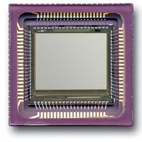
... Color Filter Array Mono RGB Bayer Pattern Packaging 84-pins LCC Cypress Semiconductor Corporation Document #: 38-05710 Rev. *A 1.3 MP CMOS Image Sensor Description The IBIS5-B-1300 is a solid state CMOS image sensor that integrates the functionality of complete analog image acqui- sition, digitizer and digital signal processing system on a single chip ...
Page 2
Architecture and Operation In this part the most important blocks of the sensor are described in more detail. Floor Plan Figure 1. Block Diagram of the IBIS5-B-1300 Image Sensor Pixel Y-left addressing Column amplifiers Analog multiplexer X-addressing Figure 1 shows ...
Page 3
Color Filter Array The IBIS5-B-1300 can also be processed with a Bayer RGB color pattern. Pixel (0,0) has a green filter and is situated on a green-blue row. Green1 and green2 have a slightly different spectral response due to cross ...
Page 4
RBT: Row Blanking Time = 3.5 ms (typical). Pixel period: 1/40 MHz = 25 ns. Example Read out time of the full resolution at nominal speed (40 MHz pixel rate) with an integration time of 1 ms: => Frame period ...
Page 5
The VDDR_RIGHT voltage is generated VDDR_LEFT voltage using a circuit that can be programmed with the KNEEPOINT_LSB/MSB bits in the sequencer register (see also “Pixel Reset Knee-point for Multiple Slope Operation (bits 8, 9, and 10).” on page 14). By ...
Page 6
X-Addressing Because of the high pixel rate, the X-shift register selects 2 columns at the time for readout runs at half the system clock speed. All even columns are connected to bus A; all odd columns to bus ...
Page 7
Y_SYNC Y_SUB DEC(n+1) DEC(n+2) DEC(n+3) DEC(n+4) Table 7. Y–Sub-sample Patterns normal mode the pointer for the pixel row is shifted one at the time. When sub-sampling is enabled, Y_SYNC is activated. The Y-shift ...
Page 8
S odd R S even + R DAC_FINE DAC_VHIGH DAC_FINE [6:0] DAC_RAW [6:0] DAC_VLOW Figure 9. In- and External DAC Connections DAC_VHIGH = 3.3V R DAC DAC_VLOW = 0V The internal resistor R has a value of approximately DAC 7.88 ...
Page 9
Due to these delays it is advised that a variable phase difference is foreseen between the ADC_CLOCK and the SYS_CLOCK to tune the optimal sample moment of the ADC. Setting of the ADC Reference Voltages Figure 11. In- and External ...
Page 10
Figure 12. Linear and Non-linear ADC Conversion Characteristic Line number Frame time Document #: 38-05710 Rev. *A Figure 13. Rolling Shutter Operation x Reset line Read line Reset sequence Time axis Integration time IBIS5-B-1300 CYII5FM1300AB Page 10 ...
Page 11
Line number Integration time Snapshot (Synchronous) Shutter A synchronous (global, snapshot) shutter solves the inconve- nience found in the rolling shutter. Light integration takes place on all pixels in parallel, although subsequent readout is sequential. Figure 14 shows the integration ...
Page 12
Table 10.Internal Registers Register Bit 0 (0000) 11:0 SEQUENCER register 0 SHUTTER_TYPE 1 FRAME_CAL_MODE 2 LINE_CAL_MODE 3 CONT_CHARGE 4 GRAN_X_SEQ_LSB 5 GRAN_X_SEQ_MSB 6 GRAN_SS_SEQ_LSB 7 GRAN_SS_SEQ_MSB 8 KNEEPOINT_LSB 9 KNEEPOINT_MSB 10 KNEEPOINT_ENABLE 11 VDDR_RIGHT_EXT 1 (0001) 11:0 NROF_PIXELS 2 (0010) ...
Page 13
Table 10.Internal Registers (continued) Register Bit 9 (1001) 6:0 DACRAW_REG 10 (1010) 6:0 DACFINE_REG 11 (1011) 2:0 ADC register 0 TRISTATE_OUT 1 GAMMA 2 BIT_INV 12 (1100) Reserved. 13 (1101) Reserved. 14 (1110) Reserved. 15 (1111) Reserved. Detailed Description of ...
Page 14
Pixel Reset Knee-point for Multiple Slope Operation (bits 8, 9, and 10). In normal (single slope) mode the pixel reset is controlled from the left side of the image core using the voltage ap- plied on pin VDDR_LEFT as ...
Page 15
X_REG Register (10:0) The X_REG register determines the start position of the window in the X-direction. In this direction, there are 640 possible starting positions (2 pixels are addressed at the same time in one clock cycle). If sub sampling ...
Page 16
Serial-3-wire Interface The serial-3-wire interface (or Serial-to-Parallel Interface) uses a serial input to shift the data in the register buffer. When the complete data word is shifted into the register buffer the data word is loaded into the internal register ...
Page 17
Timing Diagrams Timing Requirements There are 6 control signals that operate the image sensor: • SS_START • SS_STOP • Y_CLOCK • Y_START • X_LOAD • SYS_CLOCK These control signals must be generated by the external system with following time constraints ...
Page 18
Figure 22. Synchronous Shutter: Pixel Read Out Synchronous Shutter: Pixel Readout Basic Operation Y_START and Y_CLOCK must change on the falling edge of the SYS_CLOCK (Tsetup and Thold > 7.5 ns). The pulse width must be a minimum of 1 ...
Page 19
Synchronous Shutter: Multiple Slope Integration Up to four different pixel reset voltages can be used during multiple slope operation in synchronous shutter mode. This is done by uploading new values KNEEPOINT_MSB/LSB/ENABLE before a new SS_START pulse is applied. Bit KNEEPOINT_ENABLE ...
Page 20
Rolling Shutter Operation The integration of the light in the image sensor is done during readout of the other lines. The only difference with synchronous shutter is that the TIME_OUT pin is used to indicate when the Y_SYNC pulse for ...
Page 21
Windowing in Y-direction A new Y-pointer can be loaded into the Y-shift-register, by reapplying the Y_START pulse after loading a new Y-pointer value into the YL_REG and YR_REG registers. Every time a Y_START pulse appears, a frame calibration of the ...
Page 22
Pin List The IBIS5-B-1300 image sensor is packaged in a leadless ceramic carrier (LCC package). their functions. In total, there are 84 pins Table 20.Pin List Pin Pin Name Pin Type 1 P_DATA<8> ...
Page 23
Table 20.Pin List (continued) Pin Pin Name Pin Type Analog input. Biasing of the column amplifiers. Connect to VDDA with Ω and 31 COL_CMD Input decouple with C = ...
Page 24
Table 20.Pin List (continued) Pin Pin Name Pin Type 71 ADC_VDDD Supply Digital supply voltage. ADC digital supply voltage [3.3V]. 72 ADC_GNDA Ground Analog ground. ADC analog ground. 73 ADC_GNDD Ground Digital ground. ...
Page 25
Specifications General Specifications. Table 21.General Specifications Parameter Specification Pixel architecture 4T-pixel 6.7 µ 6.7 µ m Pixel size Resolution 1280 x 1024 Pixel rate 40 MHz Shutter type • Electronic rolling shutter • Snapshot shutter Full frame rate ...
Page 26
Spectral Response Curve 0.225 0.2 0.175 0.15 0.125 0.1 0.075 0.05 0.025 0 400 500 Figure 28 shows the spectral response characteristic for the IBIS5-B-1300 (CYII5SM1300AB) and the IBIS-5-BE-1300 (CYII5FM1300AB). The curve is measured directly on the pixels. It includes ...
Page 27
Electro-voltaic Response Curve 1,2 1 0,8 0,6 0,4 0 10000 20000 Figure 29 shows the pixel response curve in linear response mode. This curve is the relation between the electrons detected in the pixel and the output signal. ...
Page 28
Features and General Specifications Table 24.Features and General Specifications Feature Electronic shutter types 1. Rolling curtain shutter. 2. Synchronous (snapshot) shutter. Windowing (ROI) Implemented as scanning of lines/columns from an uploaded position. Sub-sampling modes: 1:2 sub-sampling. Sub-sampling patterns: XXOOXXOO (for ...
Page 29
Recommended Operating Conditions Table 26.Recommended Operating Conditions Parameter VDDH Voltage on HOLD switches. VDDR_LEFT Highest reset voltage. VDDC Pixel core voltage. VDDA Analog supply voltage of the image core. VDDD Digital supply voltage of the image core. GNDA Analog ground ...
Page 30
Pad position and Packaging Bare Die The IBIS5-B-1300 image sensor has 84 pins, 21 pins on every edge. The die size from pad-edge to pad-edge (without scribe-line) is: 10156.5 µm (x) by 9297.25 µm (y). Scribe lines take about 100 ...
Page 31
IBIS5-B-1300 in 84-pin LCC Package Technical Drawing of the 84-pin LCC Package Figure 31. Top View of the 84-pin LCC Package (all dimensions in mm) Figure 32. Side View of the 84-pin LCC Package (all dimensions in mm) Document #: ...
Page 32
Table 28.Side View Dimensions Dimension Description A Glass (thickness) - mono B Cavity (depth) C Die - Si (thickness) - mono D Bottom layer (thickness) E Die attach-bondline (thickness) F Glass attach-bondline (thickness) G Imager to lid-outer surface H Imager ...
Page 33
Bonding of the IBIS5-B-1300 Sensor in the 84-pin LCC Package Figure 35. Bonding of the IBIS5-B-1300 in the 84-pin LCC Package Document #: 38-05710 Rev. *A IBIS5-B-1300 CYII5FM1300AB Page [+] Feedback ...
Page 34
Die Placement of the IBIS5-B-1300 in the 84-pin LCC Package Figure 36. Die Placement of the IBIS5-B-1300 in the 84-pin LCC Package (all dimensions in mm) Tolerance on the die placement in X- and Y-directions is maximal ±50 µ m. ...
Page 35
IBIS5B in BGA Package Mechanical drawing of the BGA package Figure 37. Mechanical Drawing of the BGA Package Dimensions of the BGA package Document #: 38-05710 Rev. *A Figure 38. Dimensions of the BGA Package IBIS5-B-1300 CYII5FM1300AB Page 35 of ...
Page 36
Optical area location and ball placement Figure 39. Location of the Optical Area and Ball Placement Ball grid contact pins Document #: 38-05710 Rev. *A Figure 40. Ball Connection Matrix IBIS5-B-1300 CYII5FM1300AB Page [+] Feedback ...
Page 37
Cover Glass A D263 glass lid (which has a refraction index of 1.52) is used as a protection glass lid on top of all IBIS5-B-1300 sensors. Figure 41 shows the transmission characteristics of the D263 glass. Figure 41. Transmission Characteristics ...
Page 38
Storage and Handling Storage Conditions Table 29.Storage Conditions Description Minimum Maximum Temperature –30 +85 Handling and Soldering Conditions Special care must be taken when soldering image sensors with color filter arrays (RGB color filters) onto a circuit board since color ...
Page 39
... A case that the above material is added as a chemical com- position into the inquired product intentionally in order to Ordering Information Cypress Part number CYII5SC1300AA-HSC CYII5SC1300AB-HDC CYII5SM1300AB-HDC 84-pin JLCC CYII5SM1300AB-QDC CYII5SC1300AB-QDC CYIIFM1300AB-QDC CYII5SM1300AB-SDCES (preliminary) CYII5FM1300AB-SDCES (preliminary) Notes 6. JLCC package for use in evaluation kits only. 7. D263 is used as protective cover glass lid (see 8 ...
Page 40
For evaluating purposes an IBIS5 evaluation kit is available. The IBIS5 evaluation kit consists of a multifunctional digital board (memory, sequencer and IEEE 1394 Fire Wire interface) and an analog image sensor board. Figure 43. Content of the IBIS5 Evaluation ...
Page 41
Appendix B: IBIS5-1300 Revision Overview Table 31.IBIS5-1300 Revision Differences Parameter Status Obsolete (peak) 0.13 A/W (@ 650 nm) Full well charge 120.000 e- Output signal swing 1V (unity gain) 1.8V (max.) 12 µ V/e– Conversion gain Temporal ...
Page 42
Document History Page Document Title: IBIS5-B-1300 CYII5FM1300AB 1.3 MP CMOS Image Sensor Document Number: 38-05710 REV. ECN NO. Issue Date ** 310213 See ECN *A 649064 See ECN Document #: 38-05710 Rev. *A Orig. of Change Description of Change FVK ...