CYII5SC1300-EVAL Cypress Semiconductor Corp, CYII5SC1300-EVAL Datasheet - Page 14
CYII5SC1300-EVAL
Manufacturer Part Number
CYII5SC1300-EVAL
Description
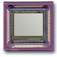
BOARD EVAL IMG SENS IBIS5-B-1300
Manufacturer
Cypress Semiconductor Corp
Specifications of CYII5SC1300-EVAL
Sensor Type
CMOS Imaging, Color (RGB)
Sensing Range
1.3 Megapixel
Interface
Parallel/Serial
Sensitivity
106 fps
Voltage - Supply
3 V ~ 4.5 V
Embedded
No
Utilized Ic / Part
IBIS5-B-1300
Lead Free Status / RoHS Status
Contains lead / RoHS non-compliant
Lead Free Status / RoHS Status
Lead free / RoHS Compliant, Contains lead / RoHS non-compliant


Document #: 38-05710 Rev. *A
Table 13.Multiple Slope Register Settings
NROF_PIXELS Register (11:0)
After the internal x_sync is generated (start of the pixel readout
of a particular row), the PIXEL_VALID signal goes high. The
PIXEL_VALID signal goes low when the pixel counter reaches
the value loaded in the NROF_PIXEL register. Due to the fact
that 2 pixels are read at the same clock cycle this number have
to be divided by 2 (NROF_PIXELS = (width of ROI / 2) – 1).
5. Pixel Reset Knee-point for Multiple Slope Operation (bits 8,
6. External Pixel Reset Voltage for Multiple Slope (bit 11)
MSB/LSB
9, and 10).
In normal (single slope) mode the pixel reset is controlled
from the left side of the image core using the voltage ap-
plied on pin VDDR_LEFT as pixel reset voltage.
In multiple slope operation one or more variable pixel reset
voltages have to be applied.
Bits KNEE_POINT_MSB and KNEE_POINT_LSB select
the on chip-generated pixel reset voltage.
Bit KNEE_POINT_ENABLE set to “1” switches control to
the right side of the image core so the pixel reset voltage
(VDDR_RIGHT),
KNEE_POINT_MSB/LSB, is used.
Bit KNEE_POINT_ENABLE should only be used for multi-
ple slope operation in synchronous shutter mode. In rolling
shutter mode, only the bits KNEE_POINT_MSB/LSB must
be used to select the second knee-point in dual slope op-
eration. The actual knee-point depends on VDDH,
VDDR_LEFT and VDDC applied to the sensor.
When bit VDDR_RIGHT_EXT is set to “1”, the circuit that
generates the variable pixel reset voltage is disabled and
the voltage externally applied to pin VDDR_RIGHT is used
as the double/multiple slope reset voltage.
When bit VDDR_RIGHT_EXT is set to “0” the variable pixel
reset voltage (used for multiple slope operation) can be
monitored on pin VDDR_RIGHT.
KNEE_POINT
00
01
10
11
ENABLE
0 or 1
shift-register
Sync of left
1
1
1
Figure 15. Synchronization of the Shift Registers in Rolling Shutter Mode
Pixel reset voltage
VDDR_LEFT – 0.76
VDDR_LEFT – 1.52
VDDR_LEFT – 2.28
(V)VDDR_RIGHT
selected
VDDR_LEFT
Line n
by
Knee-point
+ 0.76
+ 1.52
+ 2.28
(V)
0
Sync of right
shift-register
bits
ROF_LINES Register (11:0)
After the internal yl_sync is generated (start of the frame
readout with Y_START), the line counter increases with each
Y_CLOCK pulse until it reaches the value loaded in the
NROF_LINES register and an LAST_LINE pulse is generated.
INT_TIME Register (11:0)
The INT_TIME register is used to set the integration time of
the electronic shutter. The interpretation of the INT_TIME
depends on the chosen shutter type (rolling or synchronous).
1. Synchronous Shutter.
2. Rolling Shutter.
After the SS_START pulse is applied an internal counter
counts the number of SS granulated clock cycles until it
reaches the value loaded in the INT_TIME register and a
TIME_OUT pulse is generated. This TIME_OUT pulse can
be used to generate the SS_STOP pulse to stop the inte-
gration. When the INT_TIME register is used the maximum
integration time is:
TINT_MAX = 212 * 256 (maximum granularity) * (40 MHZ)
– 1 = 26.2 ms.
This maximum time can be increased if an external counter
is used to trigger SS_STOP. The minimal value that should
be loaded into the INT_TIME register is 10 (see also
nal Clock Granularities (bits 4, 5, 6 and 7).” on page
When the Y_START pulse is applied (start of the frame
readout), the sequencer generates the yl_sync pulse for
the left Y-shift register (read out Y-shift register). This loads
the left Y-shift register with the pointer loaded in YL_REG
register. At each Y_CLOCK pulse, the pointer shifts to the
next row and the integration time counter increases until it
reaches the value loaded in the INT_TIME register. At that
moment, the yr_sync pulse for the right Y-shift register is
generated which loads the right Y-shift register (reset Y-shift
register) with the pointer loaded in YR_REG register (see
Figure
sync for the left Y-shift register is asserted. Both shift regis-
ters keep moving until the next sync is asserted (Y_START
for the left Y-shift register and the sync for the right Y-shift
register is generated when the integration time counter
reaches the INT_TIME value).
Treg_int Difference between left and right pointer = value
set in the INT_TIME register (number of lines)
The actual integration time is given by:
Tint Integration time [# lines] = NROF_LINES register –
INT_TIME register
T
reg_int
15). The integration time counter is reset when the
Sync
Last line, followed by
sync of left shift-register
CYII5FM1300AB
IBIS5-B-1300
T
Page 14 of 42
int
“Inter-
13).
[+] Feedback
Related parts for CYII5SC1300-EVAL
Image
Part Number
Description
Manufacturer
Datasheet
Request
R

Part Number:
Description:
Manufacturer:
Cypress Semiconductor Corp
Datasheet:
Part Number:
Description:
Manufacturer:
Cypress Semiconductor Corp
Datasheet:
Part Number:
Description:
Manufacturer:
Cypress Semiconductor Corp
Datasheet:
Part Number:
Description:
Manufacturer:
Cypress Semiconductor Corp
Datasheet:
Part Number:
Description:
Manufacturer:
Cypress Semiconductor Corp
Datasheet: