STEVAL-IFS012V1 STMicroelectronics, STEVAL-IFS012V1 Datasheet - Page 125
STEVAL-IFS012V1
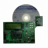
Manufacturer Part Number
STEVAL-IFS012V1
Description
BOARD ST72651AR6/STTS75/STLM20
Manufacturer
STMicroelectronics
Specifications of STEVAL-IFS012V1
Sensor Type
Temperature
Sensing Range
Depends on IC
Interface
I²C, USB
Sensitivity
Depends on IC
Voltage - Supply
5V
Embedded
Yes, MCU, 8-Bit
Utilized Ic / Part
ST72F651AR6, STTS75, STLM20
Lead Free Status / RoHS Status
Lead free / RoHS Compliant
Other names
497-8419
Available stocks
Company
Part Number
Manufacturer
Quantity
Price


13.2 ABSOLUTE MAXIMUM RATINGS
Stresses above those listed as “absolute maxi-
mum ratings” may cause permanent damage to
the device. This is a stress rating only and func-
tional operation of the device under these condi-
13.2.1 Voltage Characteristics
13.2.2 Current Characteristics
13.2.3 Thermal Characteristics
Notes:
1. Directly connecting the RESET and I/O pins to V
is generated or an unexpected change of the I/O configuration occurs (for example, due to a corrupted program counter).
To guarantee safe operation, this connection has to be done through a pull-up or pull-down resistor (typical: 4.7kΩ for
RESET, 10kΩ for I/Os). Unused I/O pins must be tied in the same way to V
2. I
respected, the injection current must be limited externally to the I
while a negative injection is induced by V
3. All power (V
4. Negative injection disturbs the analog performance of the device. In particular, it induces leakage currents throughout
the device including the analog inputs. To avoid undesirable effects on the analog functions, care must be taken:
- Analog input pins must have a negative injection less than 0.8 mA (assuming that the impedance of the analog voltage
is lower than the specified limits)
- Pure digital pins must have a negative injection less than 1.6mA. In addition, it is recommended to inject the current as
far as possible from the analog input pins.
5. When several inputs are submitted to a current injection, the maximum ΣI
and negative injected currents (instantaneous values). These results are based on characterisation with ΣI
mum current injection on four I/O port pins of the device.
6. True open drain I/O port pins do not accept positive injection.
7. Injected current on PD7 is 0 to +5mA instead of being ±5mA as with any other pin.
INJ(PIN)
I
INJ(PIN)
ΣI
V
V
V
Symbol
Symbol
Symbol
ESD(HBM)
DD
INJ(PIN)
IN
T
I
I
must never be exceeded. This is implicitly insured if V
VDD
VSS
I
STG
T
1) & 2)
IO
- V
J
2) & 4)
DD
SS
2)
) and ground (V
Supply voltage
Input voltage on any pin
Electro-static discharge voltage (Human Body Model)
Total current into V
Total current out of V
Output current sunk by any standard I/O and control pin
Output current sunk by any high sink I/O pin
Output current source by any I/Os and control pin
Injected current on
Injected current on RESET pin
Injected current on OSC1 and OSC2 pins
Injected current on any other pin
Total injected current (sum of all I/O and control pins)
Storage temperature range
Maximum junction temperature: See
SS
) lines must always be connected to the external supply.
IN
<V
DD
V
SS
PP
SS
.
power lines (source)
Ratings
Ratings
pin
Ratings
Doc ID 7215 Rev 4
ground lines (sink)
DD
or V
SS
5), 6) & 7)
could damage the device if an unintentional internal reset
tions is not implied. Exposure to maximum rating
conditions for extended periods may affect device
reliability.
section 14.2 on page 152
INJ(PIN)
IN
maximum is respected. If V
3)
3)
value. A positive injection is induced by V
DD
or V
INJ(PIN)
SS
5)
according to their reset configuration.
is the absolute sum of the positive
V
Maximum value
Maximum value
SS
-0.3 to V
-65 to +150
for T
Value
2000
± 20
- 25
100
6.0
± 5
± 5
± 5
± 5
80
25
50
Jmax
IN
DD
maximum cannot be
+0.3
ST72651AR6
INJ(PIN)
Unit
Unit
Unit
125/161
mA
°C
IN
V
maxi-
>V
DD
Related parts for STEVAL-IFS012V1
Image
Part Number
Description
Manufacturer
Datasheet
Request
R

Part Number:
Description:
BOARD EVAL SPZB260 MOD FOR STR9
Manufacturer:
STMicroelectronics
Datasheet:

Part Number:
Description:
BOARD EVAL EXTENSION SN250
Manufacturer:
STMicroelectronics
Datasheet:

Part Number:
Description:
BOARD EVAL AB-54003L-512
Manufacturer:
STMicroelectronics
Datasheet:

Part Number:
Description:
BOARD REF DESIGN RF DMOS PWR AMP
Manufacturer:
STMicroelectronics
Datasheet:

Part Number:
Description:
BOARD EVAL PWR AMP AB-84008L-470
Manufacturer:
STMicroelectronics
Datasheet:

Part Number:
Description:
BOARD EVAL FOR STM32F103XX
Manufacturer:
STMicroelectronics
Datasheet:

Part Number:
Description:
BOARD EVAL AB-54003L-512
Manufacturer:
STMicroelectronics
Datasheet:

Part Number:
Description:
BOARD SMART PLUG STM32 SPZB260PR
Manufacturer:
STMicroelectronics
Datasheet:

Part Number:
Description:
BOARD DEMO BLUETOOTH SPBT2532C2
Manufacturer:
STMicroelectronics
Datasheet:
Part Number:
Description:
ZIGBEE USB DONGLE EVAL KIT
Manufacturer:
STMicroelectronics
Datasheet:
Part Number:
Description:
STMicroelectronics [RIPPLE-CARRY BINARY COUNTER/DIVIDERS]
Manufacturer:
STMicroelectronics
Datasheet:
Part Number:
Description:
STMicroelectronics [LIQUID-CRYSTAL DISPLAY DRIVERS]
Manufacturer:
STMicroelectronics
Datasheet:

Part Number:
Description:
BOARD EVAL FOR MEMS SENSORS
Manufacturer:
STMicroelectronics
Datasheet: