NCP1351LEDGEVB ON Semiconductor, NCP1351LEDGEVB Datasheet - Page 9
NCP1351LEDGEVB
Manufacturer Part Number
NCP1351LEDGEVB
Description
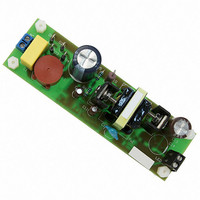
EVAL BOARD FOR NCP1351LEDG
Manufacturer
ON Semiconductor
Datasheets
1.NCP1351APG.pdf
(27 pages)
2.NCP1351LEDGEVB.pdf
(11 pages)
3.NCP1351LEDGEVB.pdf
(3 pages)
Specifications of NCP1351LEDGEVB
Design Resources
NCP1351 EVB BOM NCP1351LEDGEVB Gerber Files NCP1351LED EVB Schematic
Current - Output / Channel
700mA
Outputs And Type
1, Isolated
Voltage - Output
33V
Features
Short-Circuit Protection
Voltage - Input
85 ~ 265 V
Utilized Ic / Part
NCP1351
Core Chip
NCP1351
Topology
Flyback
No. Of Outputs
1
Output Current
700mA
Output Voltage
33V
Development Tool Type
Hardware - Eval/Demo Board
Leaded Process Compatible
Yes
Rohs Compliant
Yes
Lead Free Status / RoHS Status
Lead free / RoHS Compliant
For Use With/related Products
NCP1351LEDG
Other names
NCP1351LEDGEVBOS


technique whose regulation scheme implements a variable
switching frequency. As shown on the typical application
diagram, the controller is designed to operate with a
minimum number of external components. It incorporates
the following features:
•
•
•
•
•
•
The NCP1351 implements a fixed peak current mode
Frequency Foldback: Since the switching period
increases when power demand decreases, the switching
frequency naturally diminishes in light load conditions.
This helps to minimize switching losses and offers
good standby power performance.
Very Low Startup Current: The patented internal
supply block is specially designed to offer a very low
current consumption during startup. It allows the use of
a very high value external startup resistor, greatly
reducing dissipation, improving efficiency and
minimizing standby power consumption.
Natural Frequency Dithering: The quasi-fixed t
mode of operation improves the EMI signature since
the switching frequency varies with the natural bulk
ripple voltage.
Peak Current Compression: As the load becomes
lighter, the frequency decreases and can enter the
audible range. To avoid exciting transformer
mechanical resonances, hence generating acoustic
noise, the NCP1351 includes a patented technique,
which reduces the peak current as power goes down. As
such, inexpensive transformer can be used without
having noise problems.
Negative Primary Current Sensing: By sensing the
total current, this technique does not modify the
MOSFET driving voltage (V
Furthermore, the programming resistor, together with
the pin capacitance, forms a residual noise filter which
blanks spurious spikes.
Programmable Primary Current Sense: It offers a
second peak current adjustment variable, which
improves the design flexibility.
GS
) while switching.
http://onsemi.com
ON
NCP1351
9
•
•
•
•
•
•
Extended V
28 V, the device offers added flexibility in presence of
loosely coupled transformers. The gate drive is safely
clamped below 20 V to avoid stressing the driven
MOSFET.
Easy OPP: Connecting a resistor from the CS pin to
the auxiliary winding allows easy bulk voltage
compensation.
Secondary or Primary Regulation: The feedback
loop arrangement allows simple secondary or primary
side regulation without significant additional external
components.
Latch Input: If voltage on Pin 7 is externally brought
above 5 V, the controller permanently latches off and
stays latched until the user cycles V
V typically.
Fault Timer: In presence of badly coupled transformer,
it can be quite difficult to detect an overload or a
short-circuit on the primary side. When the feedback
current disappears, a current source charges a capacitor
connected to Pin 8. When the voltage on this pin
reaches a certain level, all pulses are shut off and the
V
This protection is latched on the A version (the
controller must be shut down and restart to resume
normal operation), and auto-recovery on Version B (if
the fault goes away, the controller automatically
resumes operation).
Dual Trip Point: in some applications, such as printer
power supplies, it is necessary to let the power supply
deliver more power on a transient event. If the event
lasts longer than what the fault timer authorizes, then
the NCP1351 either latches-off (C Version) or enters an
auto-recovery mode (D Version). The level at which
the timer starts is internally set to 55% of the maximum
power capability.
CC
voltage is pulled down below the VCC
CC
Range: By accepting V
CC
down, below 4
CC
levels up to
(min)
level.
Related parts for NCP1351LEDGEVB
Image
Part Number
Description
Manufacturer
Datasheet
Request
R

Part Number:
Description:
ON Semiconductor [VOLTAGE REGULATOR]
Manufacturer:
ON Semiconductor
Datasheet:
Part Number:
Description:
357-036-542-201 CARDEDGE 36POS DL .156 BLK LOPRO
Manufacturer:
ON Semiconductor
Datasheet:
Part Number:
Description:
357-036-542-201 CARDEDGE 36POS DL .156 BLK LOPRO
Manufacturer:
ON Semiconductor
Datasheet:
Part Number:
Description:
357-036-542-201 CARDEDGE 36POS DL .156 BLK LOPRO
Manufacturer:
ON Semiconductor
Datasheet:
Part Number:
Description:
357-036-542-201 CARDEDGE 36POS DL .156 BLK LOPRO
Manufacturer:
ON Semiconductor
Datasheet:
Part Number:
Description:
357-036-542-201 CARDEDGE 36POS DL .156 BLK LOPRO
Manufacturer:
ON Semiconductor
Datasheet:
Part Number:
Description:
357-036-542-201 CARDEDGE 36POS DL .156 BLK LOPRO
Manufacturer:
ON Semiconductor
Datasheet:
Part Number:
Description:
357-036-542-201 CARDEDGE 36POS DL .156 BLK LOPRO
Manufacturer:
ON Semiconductor
Datasheet:
Part Number:
Description:
357-036-542-201 CARDEDGE 36POS DL .156 BLK LOPRO
Manufacturer:
ON Semiconductor
Datasheet:
Part Number:
Description:
357-036-542-201 CARDEDGE 36POS DL .156 BLK LOPRO
Manufacturer:
ON Semiconductor
Datasheet:
Part Number:
Description:
357-036-542-201 CARDEDGE 36POS DL .156 BLK LOPRO
Manufacturer:
ON Semiconductor
Datasheet:
Part Number:
Description:
Manufacturer:
ON Semiconductor
Datasheet:
Part Number:
Description:
Manufacturer:
ON Semiconductor
Datasheet:
Part Number:
Description:
Manufacturer:
ON Semiconductor
Datasheet: