NCP1351LEDGEVB ON Semiconductor, NCP1351LEDGEVB Datasheet - Page 19
NCP1351LEDGEVB
Manufacturer Part Number
NCP1351LEDGEVB
Description
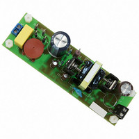
EVAL BOARD FOR NCP1351LEDG
Manufacturer
ON Semiconductor
Datasheets
1.NCP1351APG.pdf
(27 pages)
2.NCP1351LEDGEVB.pdf
(11 pages)
3.NCP1351LEDGEVB.pdf
(3 pages)
Specifications of NCP1351LEDGEVB
Design Resources
NCP1351 EVB BOM NCP1351LEDGEVB Gerber Files NCP1351LED EVB Schematic
Current - Output / Channel
700mA
Outputs And Type
1, Isolated
Voltage - Output
33V
Features
Short-Circuit Protection
Voltage - Input
85 ~ 265 V
Utilized Ic / Part
NCP1351
Core Chip
NCP1351
Topology
Flyback
No. Of Outputs
1
Output Current
700mA
Output Voltage
33V
Development Tool Type
Hardware - Eval/Demo Board
Leaded Process Compatible
Yes
Rohs Compliant
Yes
Lead Free Status / RoHS Status
Lead free / RoHS Compliant
For Use With/related Products
NCP1351LEDG
Other names
NCP1351LEDGEVBOS


Latch Input
prevents the FB input to be of low impedance before the V
reaches the VCC
a primary regulation scheme. Capitalizing on this typical
option, Figure 24 shows how to insert a zener diode in series
with the optocoupler emitter pin. In that way, the current
biases the zener diode and offers a nice reference voltage,
appearing at the loop closure (e.g. when the output reaches
the target). Yes, you can use this reference voltage to supply
a NTC and form a cheap OTP protection.
Design Example, a 19 V / 3 A
Switch-Mode Power Supply using the NCP1351 does not
differ from a fixed frequency design. What changes,
however, is the regulation method via frequency variations.
In other words, all the calculations must be carried at the
lowest line input where the frequency will hit the maximum
value set by the C
V
V
V
I
Operating mode is CCM
h = 0.8
F
out
Figure 25. You can either directly observe the V
sw
out
in
in
The NCP1351 features a patented circuitry which
R
A Universal Mains Power Supply Designing a
contribution. The best is to directly sense the output voltage and reacts if it runs away, as offered on the right
pulldown
min = 100 Vdc (bulk valley in low-line conditions)
max = 375 Vdc
= 3 A
= 65 kHz
= 19 V
1. Turn Ratio. This is the first parameter to consider.
Latch
V
CC
The MOSFET BV
of reflected voltage you need. If we consider a
600 V MOSFET and a 15% derating factor, we
must limit the maximum drain voltage to:
ON
t
capacitor. Let us follow the steps:
C3
C3
100nF
100nF
level. As such, the circuit can work in
CV
20mF
R
CC
OVP
dss
actually dictates the amount
L
aux
C4
100n
1N4937
D2
R4
2.2k
C5
1n
CC
http://onsemi.com
level or add a small RC filter to reduce the leakage inductance
CC
NCP1351
side.
19
Knowing a maximum bulk voltage of 375 V, the clamp
voltage must be set to:
Based on the above level, we decide to adopt a headroom
between the reflected voltage and the clamp level of 50 V. If
this headroom is too small, a high dissipation will occur on
the RDC clamp network and efficiency will suffer. A
leakage inductance of around 1% of the magnetizing value
should give good results with this choice (k
ratio between primary and secondary is simply:
Solving for N gives:
Figure 24. The Latch Input Offers Everything Needed
V ds_max + 600
V clamp + 510 * 375 + 135 V
N +
V out ) V f
to Implement an OTP Circuit. Another Zener Can
Latch
V
+ 0.234
C2
100n
CC
Help combining an OVP Circuit if Necessary
N s
N p
N
+
U1B
V
CC
k C V out ) V f
R1
2.5k
+
5V
V clamp
V clamp
+
k c
CV
22mF
C1
100nF
0.85 + 510 V
C1
100nF
CC
FB
Aux
+
Sec
1.6
R
pulldown
Latch
( 19 ) 0.8 )
135
+
c
= 1.6). The turn
C3
100nF
U1A
D4
OVP
(eq. 17)
(eq. 18)
(eq. 19)
(eq. 20)
OUT
D2
Related parts for NCP1351LEDGEVB
Image
Part Number
Description
Manufacturer
Datasheet
Request
R

Part Number:
Description:
ON Semiconductor [VOLTAGE REGULATOR]
Manufacturer:
ON Semiconductor
Datasheet:
Part Number:
Description:
357-036-542-201 CARDEDGE 36POS DL .156 BLK LOPRO
Manufacturer:
ON Semiconductor
Datasheet:
Part Number:
Description:
357-036-542-201 CARDEDGE 36POS DL .156 BLK LOPRO
Manufacturer:
ON Semiconductor
Datasheet:
Part Number:
Description:
357-036-542-201 CARDEDGE 36POS DL .156 BLK LOPRO
Manufacturer:
ON Semiconductor
Datasheet:
Part Number:
Description:
357-036-542-201 CARDEDGE 36POS DL .156 BLK LOPRO
Manufacturer:
ON Semiconductor
Datasheet:
Part Number:
Description:
357-036-542-201 CARDEDGE 36POS DL .156 BLK LOPRO
Manufacturer:
ON Semiconductor
Datasheet:
Part Number:
Description:
357-036-542-201 CARDEDGE 36POS DL .156 BLK LOPRO
Manufacturer:
ON Semiconductor
Datasheet:
Part Number:
Description:
357-036-542-201 CARDEDGE 36POS DL .156 BLK LOPRO
Manufacturer:
ON Semiconductor
Datasheet:
Part Number:
Description:
357-036-542-201 CARDEDGE 36POS DL .156 BLK LOPRO
Manufacturer:
ON Semiconductor
Datasheet:
Part Number:
Description:
357-036-542-201 CARDEDGE 36POS DL .156 BLK LOPRO
Manufacturer:
ON Semiconductor
Datasheet:
Part Number:
Description:
357-036-542-201 CARDEDGE 36POS DL .156 BLK LOPRO
Manufacturer:
ON Semiconductor
Datasheet:
Part Number:
Description:
Manufacturer:
ON Semiconductor
Datasheet:
Part Number:
Description:
Manufacturer:
ON Semiconductor
Datasheet:
Part Number:
Description:
Manufacturer:
ON Semiconductor
Datasheet: