NCP1351LEDGEVB ON Semiconductor, NCP1351LEDGEVB Datasheet
NCP1351LEDGEVB
Specifications of NCP1351LEDGEVB


Related parts for NCP1351LEDGEVB

NCP1351LEDGEVB Summary of contents
Page 1
Device Application NCP1351 Solid State Lighting Maximum Output Voltage Ripple Nominal Current PFC (Yes/No) Target Efficiency Max Size Operating Temp Range Cooling Method/Supply Orientation Signal Level Control Other Requirements Circuit Description The NCP1351 controller provides for a low cost, variable ...
Page 2
September 2008, Rev. 2 DN06040/D Schematic www.onsemi.com 2 ...
Page 3
LED Current The light output of an LED is determined by the forward current so the control loop will be constant current, with a simple Zener to limit the maximum output voltage. Typical forward voltages vary by LED supplier, below ...
Page 4
VALLEY I AVE δ Looking at the waveform of the current flowing in the primary of the inductor (above define a term k equal to; Δ ...
Page 5
Rectifier snubber Testing demonstrated the need for snubbing on the rectifier as there was a large amount of ringing present after the rectifier turns off. The snubber consists of a resistor and capacitor in series, and knowing the junction capacitance ...
Page 6
... ON Semiconductor Project / Customer: Part Description Transformer - Schematic ID: EE25 Core Type: Gap for 250 µH Core Gap: 250 µH Inductance: NIC 10-pin vertical Bobbin Type: Windings (in order): Winding # / type N1, Primary N2, Secondary N3, Primary N4, Primary (Aux) Sleeving and insulation between primary and secondary as required to meet the requirements of double insulation. Primary leakage inductance (pins 6& ...
Page 7
... NIC NMC1206X7R105K50F ON Semiconductor 1N4007RLG ON Semiconductor 1N4007RLG ON Semiconductor 1N4007RLG ON Semiconductor 1N4007RLG ON Semiconductor MMSD4148T1G ON Semiconductor 1SMA5932BT3G ON Semiconductor MURA160T3G ON Semiconductor MMSD4148T1G ON Semiconductor MUR840G ON Semiconductor MM3Z33VT1G ON Semiconductor NCP1351BDR2G Agilent HCPL-817-W0AE Wurth/Midcom 744 662 0027 Keystone 8718 Phoenix 1985881 Aavid 577102B00000G Aavid 577102B00000G ON Semiconductor BC847ALT1G IR IRFBC40A ...
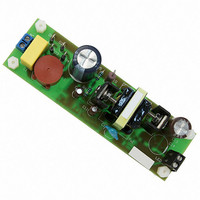
Page 8
Component Placement and PCB Layout September 2008, Rev. 2 DN06040/D Top view Bottom view Completed Demo Board, Side View www.onsemi.com 8 ...
Page 9
Turn-off in detail at 120 Vac, 230 Vac and 265 Vac September 2008, Rev. 2 DN06040/D Typical Operational Results 5 µs 100 230 120 Drain waveform at 120 Vac and ...
Page 10
Current Regulation versus Forward Voltage @ 700mA 0.8 0.7 0.6 0.5 0.4 0.3 0.2 0 3.5 7 September 2008, Rev. 2 DN06040/D Typical Evaluation Results Efficiency ...
Page 11
... Disclaimer: ON Semiconductor is providing this design note “AS IS” and does not assume any liability arising from its use; nor does ON Semiconductor convey any license to its or any third party’s intellectual property rights. This document is provided only to assist customers in evaluation of the referenced circuit implementation and the recipient assumes all liability and risk associated with its use, including, but not limited to, compliance with all regulatory standards ...