NCP1351LEDGEVB ON Semiconductor, NCP1351LEDGEVB Datasheet - Page 12
NCP1351LEDGEVB
Manufacturer Part Number
NCP1351LEDGEVB
Description
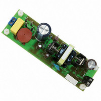
EVAL BOARD FOR NCP1351LEDG
Manufacturer
ON Semiconductor
Datasheets
1.NCP1351APG.pdf
(27 pages)
2.NCP1351LEDGEVB.pdf
(11 pages)
3.NCP1351LEDGEVB.pdf
(3 pages)
Specifications of NCP1351LEDGEVB
Design Resources
NCP1351 EVB BOM NCP1351LEDGEVB Gerber Files NCP1351LED EVB Schematic
Current - Output / Channel
700mA
Outputs And Type
1, Isolated
Voltage - Output
33V
Features
Short-Circuit Protection
Voltage - Input
85 ~ 265 V
Utilized Ic / Part
NCP1351
Core Chip
NCP1351
Topology
Flyback
No. Of Outputs
1
Output Current
700mA
Output Voltage
33V
Development Tool Type
Hardware - Eval/Demo Board
Leaded Process Compatible
Yes
Rohs Compliant
Yes
Lead Free Status / RoHS Status
Lead free / RoHS Compliant
For Use With/related Products
NCP1351LEDG
Other names
NCP1351LEDGEVBOS


few hundred Hz without any problem. The internal circuitry
naturally blocks the oscillator and softly shifts the restart
time as shown on Figure 11 scope shot.
Delays The Restart Time
sequence or a short circuit, the oscillator frequency is pushed
to the limit set by the timing capacitor. In this case, the lower
threshold imposed to the timing capacitor is blocked to
500 mV (parameter V
converter can deliver. To the opposite, as you inject current
via the optocoupler in the feedback pin, the off time expands
and the power delivery reduces. The maximum threshold
level in standby conditions is set to 6 V.
Over Power Protection
power slightly increases at high line compared to what the
In light load conditions, the frequency can go down to a
In lack of feedback current, for instance during a startup
As any universal-mains operated converters, the output
Oscillator Further Delays the Restart Time
Figure 11. In Light Load Conditions, the
Decreases
Increases
Figure 10. The Current Injected into the Feedback Loop Adjusts the Switching Frequency
P
P
out
out
fault
C
). This is the maximum power the
t
V
Voltage
Ct
Minimum Frequency
Maximum Frequency
I
Ct
= 10 mA
http://onsemi.com
NCP1351
12
power supply can deliver at low line. This discrepancy
relates to the propagation delay from the point where the
peak is detected to the MOSFET gate effective pulldown. It
naturally includes the controller reaction time, but also the
driver capability to pull the gate down. If the MOSFET Q
is too large, then this parameter will greatly affect your
overpower parameter. Sometimes, the small PNP can help
and we recommend it if you use a large Q
GND
DRV
Figure 13. A Low-Cost PNP Improves the Drive
Figure 12. C
Capability at Turn-off
t
Voltage Swing at a Moderate
D1
1N4148
C
Loading
t
Voltage
Q1
2N2907
Controlled by the
FB Current
g
MOSFET:
g
Related parts for NCP1351LEDGEVB
Image
Part Number
Description
Manufacturer
Datasheet
Request
R

Part Number:
Description:
ON Semiconductor [VOLTAGE REGULATOR]
Manufacturer:
ON Semiconductor
Datasheet:
Part Number:
Description:
357-036-542-201 CARDEDGE 36POS DL .156 BLK LOPRO
Manufacturer:
ON Semiconductor
Datasheet:
Part Number:
Description:
357-036-542-201 CARDEDGE 36POS DL .156 BLK LOPRO
Manufacturer:
ON Semiconductor
Datasheet:
Part Number:
Description:
357-036-542-201 CARDEDGE 36POS DL .156 BLK LOPRO
Manufacturer:
ON Semiconductor
Datasheet:
Part Number:
Description:
357-036-542-201 CARDEDGE 36POS DL .156 BLK LOPRO
Manufacturer:
ON Semiconductor
Datasheet:
Part Number:
Description:
357-036-542-201 CARDEDGE 36POS DL .156 BLK LOPRO
Manufacturer:
ON Semiconductor
Datasheet:
Part Number:
Description:
357-036-542-201 CARDEDGE 36POS DL .156 BLK LOPRO
Manufacturer:
ON Semiconductor
Datasheet:
Part Number:
Description:
357-036-542-201 CARDEDGE 36POS DL .156 BLK LOPRO
Manufacturer:
ON Semiconductor
Datasheet:
Part Number:
Description:
357-036-542-201 CARDEDGE 36POS DL .156 BLK LOPRO
Manufacturer:
ON Semiconductor
Datasheet:
Part Number:
Description:
357-036-542-201 CARDEDGE 36POS DL .156 BLK LOPRO
Manufacturer:
ON Semiconductor
Datasheet:
Part Number:
Description:
357-036-542-201 CARDEDGE 36POS DL .156 BLK LOPRO
Manufacturer:
ON Semiconductor
Datasheet:
Part Number:
Description:
Manufacturer:
ON Semiconductor
Datasheet:
Part Number:
Description:
Manufacturer:
ON Semiconductor
Datasheet:
Part Number:
Description:
Manufacturer:
ON Semiconductor
Datasheet: