NCP1351LEDGEVB ON Semiconductor, NCP1351LEDGEVB Datasheet - Page 13
NCP1351LEDGEVB
Manufacturer Part Number
NCP1351LEDGEVB
Description
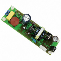
EVAL BOARD FOR NCP1351LEDG
Manufacturer
ON Semiconductor
Datasheets
1.NCP1351APG.pdf
(27 pages)
2.NCP1351LEDGEVB.pdf
(11 pages)
3.NCP1351LEDGEVB.pdf
(3 pages)
Specifications of NCP1351LEDGEVB
Design Resources
NCP1351 EVB BOM NCP1351LEDGEVB Gerber Files NCP1351LED EVB Schematic
Current - Output / Channel
700mA
Outputs And Type
1, Isolated
Voltage - Output
33V
Features
Short-Circuit Protection
Voltage - Input
85 ~ 265 V
Utilized Ic / Part
NCP1351
Core Chip
NCP1351
Topology
Flyback
No. Of Outputs
1
Output Current
700mA
Output Voltage
33V
Development Tool Type
Hardware - Eval/Demo Board
Leaded Process Compatible
Yes
Rohs Compliant
Yes
Lead Free Status / RoHS Status
Lead free / RoHS Compliant
For Use With/related Products
NCP1351LEDG
Other names
NCP1351LEDGEVBOS


dissipation penalty by arranging components around the
auxiliary as suggested by Figure 14. On this schematic, the
diode anode swings negative during the on time. This
negative level directly depends on the input voltage and
offsets the current sense pin via the R
integration is necessary to reduce the O
conditions. However, depending on the compensation level,
15% in high-line conditions. The turn-ratio between the
auxiliary winding and the primary winding is N
its value is 0.15. Thus, the voltage on D
negative during the on time to a level of:
If we selected a 3.7 kW resistor for R
maximum sense voltage being developed is:
The small RC network made of R
the voltage excursion on D
inductance value gives an on time of 3 ms at high-line. The
voltage across C
V aux_peak + -V in_max N aux + -375
V sense + 3.7 k
V C 3 +
Over power protection can be done without power
Suppose you would need to reduce the peak current by
t on V aux_peak
+
C
R 1 C 3
Bulk
3
thus swings down to:
Figure 14. The OPP is Relatively Easy to Implement and It Does not Waste Power
270 m + 1 V
+ -
CS
2
150 k
anode. Assume the primary
R
3 m
offset
1
and C
C4
22p
OPP
PP
270 p
56
aux
3
action in light load
, purposely limits
resistor. A small
offset
cathode swings
0.15 + -56 V
+ -4.2 V
aux
, then the
R
R
100k
. Assume
sense
OPP
(eq. 8)
(eq. 9)
http://onsemi.com
V
DRV
CC
(eq.
10)
NCP1351
13
the standby power can be affected. Again, the resistor R
should be placed as close as possible to the CS pin. The
22 pF can help to circumvent any picked-up noise and D
prevents the positive loading of the 270 pF capacitor during
the flyback swing. We have put a typical 100 kW O
resistor but a tweak is required depending on your
application.
Typically, we measured around –4 V on our 50 W prototype.
By calculation, we want to decrease the peak current by
15%. Compared to the internal 270 mA source, we need to
derive:
Thus, from the –4 V excursion, the R
derived by:
After experimental measurements, the resistor was
normalized down to 100 kW.
Feedback
works in current rather than voltage. Figure 15 details the
internal circuitry of this particular section. The optocoupler
injects a current into the FB pin in relationship with the
input/output conditions.
I offset + -0.15
R OPP +
Unlike other controllers, the feedback in the NCP1351
+
CV
D
aux
CC
1N4148
40.5 m
4
D2
+ 98 kW
L
aux
270 m + -40.5 mA
DRV
R1
150k
C3
270p
L
P
OPP
I
Lp
resistor is
(eq. 12)
(eq. 11)
OPP
PP
2
Related parts for NCP1351LEDGEVB
Image
Part Number
Description
Manufacturer
Datasheet
Request
R

Part Number:
Description:
ON Semiconductor [VOLTAGE REGULATOR]
Manufacturer:
ON Semiconductor
Datasheet:
Part Number:
Description:
357-036-542-201 CARDEDGE 36POS DL .156 BLK LOPRO
Manufacturer:
ON Semiconductor
Datasheet:
Part Number:
Description:
357-036-542-201 CARDEDGE 36POS DL .156 BLK LOPRO
Manufacturer:
ON Semiconductor
Datasheet:
Part Number:
Description:
357-036-542-201 CARDEDGE 36POS DL .156 BLK LOPRO
Manufacturer:
ON Semiconductor
Datasheet:
Part Number:
Description:
357-036-542-201 CARDEDGE 36POS DL .156 BLK LOPRO
Manufacturer:
ON Semiconductor
Datasheet:
Part Number:
Description:
357-036-542-201 CARDEDGE 36POS DL .156 BLK LOPRO
Manufacturer:
ON Semiconductor
Datasheet:
Part Number:
Description:
357-036-542-201 CARDEDGE 36POS DL .156 BLK LOPRO
Manufacturer:
ON Semiconductor
Datasheet:
Part Number:
Description:
357-036-542-201 CARDEDGE 36POS DL .156 BLK LOPRO
Manufacturer:
ON Semiconductor
Datasheet:
Part Number:
Description:
357-036-542-201 CARDEDGE 36POS DL .156 BLK LOPRO
Manufacturer:
ON Semiconductor
Datasheet:
Part Number:
Description:
357-036-542-201 CARDEDGE 36POS DL .156 BLK LOPRO
Manufacturer:
ON Semiconductor
Datasheet:
Part Number:
Description:
357-036-542-201 CARDEDGE 36POS DL .156 BLK LOPRO
Manufacturer:
ON Semiconductor
Datasheet:
Part Number:
Description:
Manufacturer:
ON Semiconductor
Datasheet:
Part Number:
Description:
Manufacturer:
ON Semiconductor
Datasheet:
Part Number:
Description:
Manufacturer:
ON Semiconductor
Datasheet: