NCP1351LEDGEVB ON Semiconductor, NCP1351LEDGEVB Datasheet - Page 14
NCP1351LEDGEVB
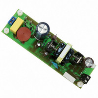
Manufacturer Part Number
NCP1351LEDGEVB
Description
EVAL BOARD FOR NCP1351LEDG
Manufacturer
ON Semiconductor
Datasheets
1.NCP1351APG.pdf
(27 pages)
2.NCP1351LEDGEVB.pdf
(11 pages)
3.NCP1351LEDGEVB.pdf
(3 pages)
Specifications of NCP1351LEDGEVB
Design Resources
NCP1351 EVB BOM NCP1351LEDGEVB Gerber Files NCP1351LED EVB Schematic
Current - Output / Channel
700mA
Outputs And Type
1, Isolated
Voltage - Output
33V
Features
Short-Circuit Protection
Voltage - Input
85 ~ 265 V
Utilized Ic / Part
NCP1351
Core Chip
NCP1351
Topology
Flyback
No. Of Outputs
1
Output Current
700mA
Output Voltage
33V
Development Tool Type
Hardware - Eval/Demo Board
Leaded Process Compatible
Yes
Rohs Compliant
Yes
Lead Free Status / RoHS Status
Lead free / RoHS Compliant
For Use With/related Products
NCP1351LEDG
Other names
NCP1351LEDGEVBOS


by the optocoupler current. The feedback current, I
Figure 15, enter an internal 45 kW resistor which develops
a voltage. This voltage becomes the variable threshold point
for the capacitor charge, as indicated by Figure 10. Thus, in
lack of feedback current (start-up or short-circuit), there is
no voltage across the 45 kW and the series offset of 500 mV
clamps the capacitor swing. If a 270 pF capacitor is used, the
maximum switching frequency is 65 kHz.
can obviously generate audible noise. For this reason, the
NCP1351 uses a patented current compression technique
which reduces the peak current in lighter load conditions. By
design, the peak current changes from 100% of its full load
value, to 30% of this value in light load conditions. This is
the block placed on the lower left corner of Figure 15. In full
The FB pin can actually be seen as a diode, forward biased
Folding the frequency back at a rather high peak current
to R
sense
22pF
C1
100n
R
3.9k
C
270p
C3
offset
t
V
CC
R1
2.5k
C
t
CS
FB
V
Figure 15. The Feedback Section Inside the NCP1351
CC
I
V
FB
CC
IC
10m
I
diff
t
ICS
= ICS
Reset
min
max
D
- ICS
FB
http://onsemi.com
FB
min
NCP1351
on
14
I
diff
I CS + I CS_min ) I dif + I CS_max * I CS_min ) I CS_min
load conditions, the feedback current is weak and all the
current flowing through the external offset resistor is:
As the load goes lighter, the feedback current increases and
starts to steal current away from the generators. Equation 12
can thus be updated by:
Equation 13 testifies for the current reduction on the offset
generator, k represents an internal coefficient. When the
feedback current equals I
I CS + I CS_max * kI FB
I CS + I CS_min
+ I CS_max
I
FB
I
FB
R
45k
FB
500mV
V
offset
I
diff
+
dif
f
(IFB)
, the offset becomes:
-
+
Clock
(eq. 13)
(eq. 14)
(eq. 15)
Related parts for NCP1351LEDGEVB
Image
Part Number
Description
Manufacturer
Datasheet
Request
R

Part Number:
Description:
ON Semiconductor [VOLTAGE REGULATOR]
Manufacturer:
ON Semiconductor
Datasheet:
Part Number:
Description:
357-036-542-201 CARDEDGE 36POS DL .156 BLK LOPRO
Manufacturer:
ON Semiconductor
Datasheet:
Part Number:
Description:
357-036-542-201 CARDEDGE 36POS DL .156 BLK LOPRO
Manufacturer:
ON Semiconductor
Datasheet:
Part Number:
Description:
357-036-542-201 CARDEDGE 36POS DL .156 BLK LOPRO
Manufacturer:
ON Semiconductor
Datasheet:
Part Number:
Description:
357-036-542-201 CARDEDGE 36POS DL .156 BLK LOPRO
Manufacturer:
ON Semiconductor
Datasheet:
Part Number:
Description:
357-036-542-201 CARDEDGE 36POS DL .156 BLK LOPRO
Manufacturer:
ON Semiconductor
Datasheet:
Part Number:
Description:
357-036-542-201 CARDEDGE 36POS DL .156 BLK LOPRO
Manufacturer:
ON Semiconductor
Datasheet:
Part Number:
Description:
357-036-542-201 CARDEDGE 36POS DL .156 BLK LOPRO
Manufacturer:
ON Semiconductor
Datasheet:
Part Number:
Description:
357-036-542-201 CARDEDGE 36POS DL .156 BLK LOPRO
Manufacturer:
ON Semiconductor
Datasheet:
Part Number:
Description:
357-036-542-201 CARDEDGE 36POS DL .156 BLK LOPRO
Manufacturer:
ON Semiconductor
Datasheet:
Part Number:
Description:
357-036-542-201 CARDEDGE 36POS DL .156 BLK LOPRO
Manufacturer:
ON Semiconductor
Datasheet:
Part Number:
Description:
Manufacturer:
ON Semiconductor
Datasheet:
Part Number:
Description:
Manufacturer:
ON Semiconductor
Datasheet:
Part Number:
Description:
Manufacturer:
ON Semiconductor
Datasheet: