RDK-91 Power Integrations, RDK-91 Datasheet - Page 8
RDK-91
Manufacturer Part Number
RDK-91
Description
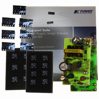
KIT DESIGN REF TINYSWITCH-III
Manufacturer
Power Integrations
Series
TinySwitch®-IIIr
Specifications of RDK-91
Main Purpose
AC/DC, Primary Side
Outputs And Type
1, Non-Isolated
Power - Output
12W
Voltage - Output
12V
Current - Output
1A
Voltage - Input
85 ~ 265VAC
Regulator Topology
Flyback
Board Type
Fully Populated
Utilized Ic / Part
TNY274, TNY275, TNY276, TNY277, TNY278, TNY279, TNY280
Product
Accessories & Kits
Lead Free Status / RoHS Status
Lead free / RoHS Compliant
Frequency - Switching
-
Other names
596-1194


4 Circuit Description
This flyback power supply was designed around the TNY278PN (U1 in Figure 2). The
output voltage is sensed and fed back to U1 through optocoupler U2. That feedback is
used by U1 to maintain constant voltage (CV) regulation of the output.
4.1 Input Rectification and Filtering
Diodes D1–D4 rectify the AC input.
Inductor L1, C1 and C2 form a pi filter that attenuates differential mode conducted EMI.
4.2 TNY278PN Operation
The TNY278PN device (U1) integrates an oscillator, a switch controller, startup and
protection circuitry, and a power MOSFET, all on one monolithic IC.
One side of the power transformer (T1) primary winding is connected to the positive leg
of C2, and the other side is connected to the DRAIN pin of U1. At the start of a switching
cycle, the controller turns the MOSFET on, and current ramps up in the primary winding,
which stores energy in the core of the transformer. When that current reaches the limit
threshold, the controller turns the MOSFET off. Due to the phasing of the transformer
windings and the orientation of the output diode, the stored energy then induces a
voltage across the secondary winding, which forward biases the output diode, and the
stored energy is delivered to the output capacitor. When the MOSFET turns off, the
leakage inductance of the transformer induces a voltage spike on the drain node. The
amplitude of that spike is limited by an RCD clamp network that consists of D5, C4 and
R2. Resistor R1 and VR1 provide hard clamping of the drain voltage, only conducting
during output overload. Resistor R2 also limits the reverse current that flows through D5
when the MOSFET turns on. This allows a slow, low-cost, glass passivated diode (with a
recovery time of ≤2 µs.) to be used for D5, which improves conducted EMI and efficiency.
Using ON/OFF control, U1 skips switching cycles to regulate the output voltage, based
on feedback to its EN/UV pin. The EN/UV pin current is sampled, just prior to each
switching cycle, to determine if that switching cycle should be enabled or disabled. If the
EN/UV pin current is <115 µA, the next switching cycle begins, and is terminated when
the current through the MOSFET reaches the internal current limit threshold. To evenly
spread switching cycles, preventing group pulsing, the EN pin threshold current is
modulated between 115 µA and 60 µA based on the state during the previous cycle. A
state-machine within the controller adjusts the MOSFET current limit threshold to one of
four levels, depending on the load being demanded from the supply. As the load on the
supply drops, the current limit threshold is reduced. This ensures that the effective
switching frequency stays above the audible range until the transformer flux density is
low.
transformer, audible noise is practically eliminated.
When the standard production technique of dip varnishing is used for the
Power Integrations
Tel: +1 408 414 9200 Fax: +1 408 414 9201
www.powerint.com
Capacitors C1 and C2 filter the rectified DC.
Page 8 of 37
Related parts for RDK-91
Image
Part Number
Description
Manufacturer
Datasheet
Request
R

Part Number:
Description:
KIT REF DESIGN 36-72W MOTOR DRVR
Manufacturer:
Power Integrations
Datasheet:

Part Number:
Description:
KIT REF DESIGN FOR LNK457D
Manufacturer:
Power Integrations
Datasheet:

Part Number:
Description:
REFERENCE DESIGN LINKSWITCH-PH
Manufacturer:
Power Integrations
Datasheet:

Part Number:
Description:
Specifications: Manufacturer: Power Integrations ; Output Voltage: 380 VDC ; Input / Supply Voltage (Max): 264 VAC ; Input / Supply Voltage (Min): 90 VAC ; Mounting Style: Through Hole ; Output Current: 0.913 A ; Output Power: 347 W
Manufacturer:
Power Integrations, Inc.

Part Number:
Description:
KIT REF DESIGN TOP HX FOR TOP258
Manufacturer:
Power Integrations
Datasheet:

Part Number:
Description:
Power Management Modules & Development Tools TOPSwitch-JX REF. DESIGN KIT
Manufacturer:
Power Integrations
Datasheet:
Part Number:
Description:
Power Management IC Development Tools REF DESIGN RDR-292 PFF LED STREET LIGHT
Manufacturer:
Power Integrations

Part Number:
Description:
KIT REF DESIGN FOR LNK403EG
Manufacturer:
Power Integrations
Datasheet:

Part Number:
Description:
KIT REF DESIGN FOR LNK406EG
Manufacturer:
Power Integrations
Datasheet:

Part Number:
Description:
KIT REF DESIGN DG CAPZERO
Manufacturer:
Power Integrations
Datasheet:

Part Number:
Description:
KIT REF DESIGN LINKSWITCH-CV
Manufacturer:
Power Integrations
Datasheet:

Part Number:
Description:
KIT REF DESIGN LINKSWITCH 2
Manufacturer:
Power Integrations
Datasheet:

Part Number:
Description:
KIT REF DESIGN PFS762HG
Manufacturer:
Power Integrations
Datasheet:
Part Number:
Description:
Specifications: Family: Eval Boards - DC/DC & AC/DC (Off-Line) SMPS ; Series: HiperLCS™ ; Main Purpose: DC/DC, Step Down ; Outputs and Type: 1, Isolated ; Power - Output: 150W ; Voltage - Output: 24V ; Current - Output: 6.25A ; Voltage - Input:
Manufacturer:
Power Integrations, Inc.
Datasheet:

Part Number:
Description:
KIT REF DESIGN 1.2W PS TN FAMILY
Manufacturer:
Power Integrations
Datasheet: