SOUNDBITE Freescale Semiconductor, SOUNDBITE Datasheet - Page 33
SOUNDBITE
Manufacturer Part Number
SOUNDBITE
Description
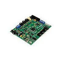
BOARD DEMO AUDIO DEVELOPMENT
Manufacturer
Freescale Semiconductor
Series
Symphony™ soundBiter
Datasheet
1.DSPB56371AF180.pdf
(68 pages)
Specifications of SOUNDBITE
Main Purpose
Audio, Audio Processing
Utilized Ic / Part
DSPB56371
Primary Attributes
Up to 8 channels of digital audio
Secondary Attributes
USB, I2C, SPI Interface
Processor To Be Evaluated
DSP56371
Data Bus Width
24 bit
Interface Type
USB
Lead Free Status / RoHS Status
Lead free / RoHS Compliant
Embedded
-
Lead Free Status / Rohs Status
Lead free / RoHS Compliant


3.13 JTAG/OnCE Interface
4
Freescale Semiconductor
Signal
This device contains circuitry protecting against damage due to high static voltage or
electrical fields. However, normal precautions should be taken to avoid exceeding
maximum voltage ratings. Reliability of operation is enhanced if unused inputs are pulled
to an appropriate logic voltage level (for example, either GND or V
value for a pull-up or pull-down resistor is 4.7 kΩ.
In the calculation of timing requirements, adding a maximum value of one specification to
a minimum value of another specification does not yield a reasonable sum. A maximum
specification is calculated using a worst case variation of process parameter values in one
direction. The minimum specification is calculated using the worst case for the same
parameters in the opposite direction. Therefore, a “maximum” value for a specification will
never occur in the same device that has a “minimum” value for another specification;
adding a maximum to a minimum represents a condition that can never exist.
Name
TDO
TMS
TCK
TDI
Maximum Ratings
Signal
Output
Type
Input
Input
Input
Tri-state
during
Reset
State
Input
Input
Input
Test Clock—TCK is a test clock input signal used to synchronize the JTAG
test logic. It has an internal pull-up resistor.
Internal Pull up resistor.
This input is 5 V tolerant.
Test Data Input—TDI is a test data serial input signal used for test instructions
and data. TDI is sampled on the rising edge of TCK and has an internal pull-up
resistor.
Internal Pull up resistor.
This input is 5 V tolerant.
Test Data Output—TDO is a test data serial output signal used for test
instructions and data. TDO is tri-statable and is actively driven in the shift-IR
and shift-DR controller states. TDO changes on the falling edge of TCK.
Test Mode Select—TMS is an input signal used to sequence the test
controller’s state machine. TMS is sampled on the rising edge of TCK and has
an internal pull-up resistor.
Internal Pull up resistor.
This input is 5 V tolerant.
Table 13. JTAG/OnCE Interface
DSP56371 Data Sheet, Rev. 4.1
CAUTION
NOTE
Signal Description
DD
). The suggested
Maximum Ratings
33
Related parts for SOUNDBITE
Image
Part Number
Description
Manufacturer
Datasheet
Request
R

Part Number:
Description:
Manufacturer:
Freescale Semiconductor, Inc
Datasheet:
Part Number:
Description:
Manufacturer:
Freescale Semiconductor, Inc
Datasheet:
Part Number:
Description:
Manufacturer:
Freescale Semiconductor, Inc
Datasheet:
Part Number:
Description:
Manufacturer:
Freescale Semiconductor, Inc
Datasheet:
Part Number:
Description:
Manufacturer:
Freescale Semiconductor, Inc
Datasheet:
Part Number:
Description:
Manufacturer:
Freescale Semiconductor, Inc
Datasheet:
Part Number:
Description:
Manufacturer:
Freescale Semiconductor, Inc
Datasheet:
Part Number:
Description:
Manufacturer:
Freescale Semiconductor, Inc
Datasheet:
Part Number:
Description:
Manufacturer:
Freescale Semiconductor, Inc
Datasheet:
Part Number:
Description:
Manufacturer:
Freescale Semiconductor, Inc
Datasheet:
Part Number:
Description:
Manufacturer:
Freescale Semiconductor, Inc
Datasheet:
Part Number:
Description:
Manufacturer:
Freescale Semiconductor, Inc
Datasheet:
Part Number:
Description:
Manufacturer:
Freescale Semiconductor, Inc
Datasheet:
Part Number:
Description:
Manufacturer:
Freescale Semiconductor, Inc
Datasheet:
Part Number:
Description:
Manufacturer:
Freescale Semiconductor, Inc
Datasheet: