SOUNDBITE Freescale Semiconductor, SOUNDBITE Datasheet - Page 14
SOUNDBITE
Manufacturer Part Number
SOUNDBITE
Description
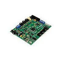
BOARD DEMO AUDIO DEVELOPMENT
Manufacturer
Freescale Semiconductor
Series
Symphony™ soundBiter
Datasheet
1.DSPB56371AF180.pdf
(68 pages)
Specifications of SOUNDBITE
Main Purpose
Audio, Audio Processing
Utilized Ic / Part
DSPB56371
Primary Attributes
Up to 8 channels of digital audio
Secondary Attributes
USB, I2C, SPI Interface
Processor To Be Evaluated
DSP56371
Data Bus Width
24 bit
Interface Type
USB
Lead Free Status / RoHS Status
Lead free / RoHS Compliant
Embedded
-
Lead Free Status / Rohs Status
Lead free / RoHS Compliant


Signal/Connection Descriptions
3.3
3.4
3.5
14
CORE_GND (4) Core Ground—The Core ground should be provided with an extremely low-impedance path to
PINIT/NMI
Ground Name
PLLD_GND(1) PLL Ground—The PLL ground should be provided with an extremely low-impedance path to
PLLA_GND(1)
PLLP_GND(1)
IO_GND (5)
EXTAL
Signal
Signal
SCAN
Name
Name
Ground
SCAN
Clock and PLL
Type
Input
Type
Input
Input
PLL Ground—The PLL ground should be provided with an extremely low-impedance path to
ground. The user must provide adequate external decoupling capacitors.
ground. The user must provide adequate external decoupling capacitors.
ground. This connection must be tied externally to all other chip ground connections. The user must
provide adequate external decoupling capacitors.
SHI, ESAI, ESAI_1, DAX and Timer I/O Ground—IO_GND is an isolated ground for the SHI, ESAI,
ESAI_1, DAX and Timer I/O. This connection must be tied externally to all other chip ground
connections. The user must provide adequate external decoupling capacitors.
During
during
Reset
Reset
State
State
Input
Input
Input
SCAN—Manufacturing test pin. This pin should be pulled low.
Internal Pull down resistor.
External Clock Input—An external clock source must be connected to EXTAL in
order to supply the clock to the internal clock generator and PLL.
This input is 5 V tolerant.
PLL Initial/Nonmaskable Interrupt—During assertion of RESET, the value of
PINIT/NMI is written into the PLL Enable (PEN) bit of the PLL control register,
determining whether the PLL is enabled or disabled. After RESET de assertion
and during normal instruction processing, the PINIT/NMI Schmitt-trigger input is
a negative-edge-triggered nonmaskable interrupt (NMI) request internally
synchronized to internal system clock.
Internal Pull up resistor.
This input is 5 V tolerant.
Table 5. Clock and PLL Signals
DSP56371 Data Sheet, Rev. 4.1
Table 4. SCAN Signals
Table 3. Grounds
Description
Signal Description
Signal Description
Freescale Semiconductor
Related parts for SOUNDBITE
Image
Part Number
Description
Manufacturer
Datasheet
Request
R

Part Number:
Description:
Manufacturer:
Freescale Semiconductor, Inc
Datasheet:
Part Number:
Description:
Manufacturer:
Freescale Semiconductor, Inc
Datasheet:
Part Number:
Description:
Manufacturer:
Freescale Semiconductor, Inc
Datasheet:
Part Number:
Description:
Manufacturer:
Freescale Semiconductor, Inc
Datasheet:
Part Number:
Description:
Manufacturer:
Freescale Semiconductor, Inc
Datasheet:
Part Number:
Description:
Manufacturer:
Freescale Semiconductor, Inc
Datasheet:
Part Number:
Description:
Manufacturer:
Freescale Semiconductor, Inc
Datasheet:
Part Number:
Description:
Manufacturer:
Freescale Semiconductor, Inc
Datasheet:
Part Number:
Description:
Manufacturer:
Freescale Semiconductor, Inc
Datasheet:
Part Number:
Description:
Manufacturer:
Freescale Semiconductor, Inc
Datasheet:
Part Number:
Description:
Manufacturer:
Freescale Semiconductor, Inc
Datasheet:
Part Number:
Description:
Manufacturer:
Freescale Semiconductor, Inc
Datasheet:
Part Number:
Description:
Manufacturer:
Freescale Semiconductor, Inc
Datasheet:
Part Number:
Description:
Manufacturer:
Freescale Semiconductor, Inc
Datasheet:
Part Number:
Description:
Manufacturer:
Freescale Semiconductor, Inc
Datasheet: