SI5356-EVB Silicon Laboratories Inc, SI5356-EVB Datasheet - Page 4
SI5356-EVB
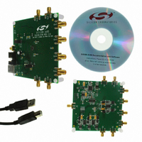
Manufacturer Part Number
SI5356-EVB
Description
EVALUATION BOARD FOR SI5356
Manufacturer
Silicon Laboratories Inc
Specifications of SI5356-EVB
Main Purpose
Timing, Clock Generator
Utilized Ic / Part
SI5356
Technology Type
Evaluation Board
For Use With/related Products
Si5356
Lead Free Status / RoHS Status
Lead free / RoHS Compliant
Secondary Attributes
-
Embedded
-
Primary Attributes
-
Lead Free Status / Rohs Status
Lead free / RoHS Compliant
Other names
336-1750


Si5356
1. Electrical Specifications
4
Table 1. Recommended Operating Conditions
(V
Table 2. Absolute Maximum Ratings
Supply Voltage Range
Input Voltage Range (all pins except pins 1,2,5,6)
Input Voltage Range (pins 1,2,5,6)
Output Voltage Range
Storage Temperature Range
ESD Tolerance
Latch-up Tolerance
Soldering Temperature (Pb-free profile)
Notes:
Ambient Temperature
Core Supply Voltage
Output Buffer Supply Voltage
Note: All minimum and maximum specifications are guaranteed and apply across the recommended operating
DD
1.
2.
= 1.8 V –5% to +10%, 2.5 or 3.3 V ±10%, T
conditions. Typical values apply at nominal supply voltages and an operating temperature of 25 °C unless
otherwise noted.
Permanent device damage may occur if the Absolute Maximum Ratings are exceeded. Functional
operation should be restricted to the conditions as specified in the operational sections of this data sheet.
Exposure to maximum rating conditions for extended periods may affect device reliability.
The device is compliant with JEDEC J-STD-020C.
Parameter
Parameter
Symbol
V
2
V
DDO
T
DD
A
1
A
= –40 to 85 °C)
Preliminary Rev. 0.3
Test Condition
Symbol
T
HBM
CDM
V
MM
PEAK
V
V
LU
T
V
DD
I2
O
S
I
2.97
2.25
1.71
1.71
Min
–40
–0.5 to V
–0.5 to +3.8
–55 to +150
–0.5 to 3.8
–0.5 to 1.2
Rating
JESD78 Compliant
550
175
260
Typ
3.3
2.5
1.8
2.5
—
—
DD
+ 0.3
Max
3.63
2.75
1.98
3.63
85
Units
Units
o
kV
o
V
V
V
V
V
V
o
C
C
V
V
C
Related parts for SI5356-EVB
Image
Part Number
Description
Manufacturer
Datasheet
Request
R

Part Number:
Description:
SMD/C°/SINGLE-ENDED OUTPUT SILICON OSCILLATOR
Manufacturer:
Silicon Laboratories Inc
Part Number:
Description:
Manufacturer:
Silicon Laboratories Inc
Datasheet:
Part Number:
Description:
N/A N/A/SI4010 AES KEYFOB DEMO WITH LCD RX
Manufacturer:
Silicon Laboratories Inc
Datasheet:
Part Number:
Description:
N/A N/A/SI4010 SIMPLIFIED KEY FOB DEMO WITH LED RX
Manufacturer:
Silicon Laboratories Inc
Datasheet:
Part Number:
Description:
N/A/-40 TO 85 OC/EZLINK MODULE; F930/4432 HIGH BAND (REV E/B1)
Manufacturer:
Silicon Laboratories Inc
Part Number:
Description:
EZLink Module; F930/4432 Low Band (rev e/B1)
Manufacturer:
Silicon Laboratories Inc
Part Number:
Description:
I°/4460 10 DBM RADIO TEST CARD 434 MHZ
Manufacturer:
Silicon Laboratories Inc
Part Number:
Description:
I°/4461 14 DBM RADIO TEST CARD 868 MHZ
Manufacturer:
Silicon Laboratories Inc
Part Number:
Description:
I°/4463 20 DBM RFSWITCH RADIO TEST CARD 460 MHZ
Manufacturer:
Silicon Laboratories Inc
Part Number:
Description:
I°/4463 20 DBM RADIO TEST CARD 868 MHZ
Manufacturer:
Silicon Laboratories Inc
Part Number:
Description:
I°/4463 27 DBM RADIO TEST CARD 868 MHZ
Manufacturer:
Silicon Laboratories Inc
Part Number:
Description:
I°/4463 SKYWORKS 30 DBM RADIO TEST CARD 915 MHZ
Manufacturer:
Silicon Laboratories Inc
Part Number:
Description:
N/A N/A/-40 TO 85 OC/4463 RFMD 30 DBM RADIO TEST CARD 915 MHZ
Manufacturer:
Silicon Laboratories Inc
Part Number:
Description:
I°/4463 20 DBM RADIO TEST CARD 169 MHZ
Manufacturer:
Silicon Laboratories Inc