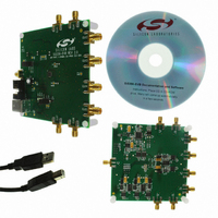
SI5356-EVB Silicon Laboratories Inc, SI5356-EVB Datasheet - Page 18

SI5356-EVB
Manufacturer Part Number
SI5356-EVB
Description
EVALUATION BOARD FOR SI5356
Manufacturer
Silicon Laboratories Inc
Specifications of SI5356-EVB
Main Purpose
Timing, Clock Generator
Utilized Ic / Part
SI5356
Technology Type
Evaluation Board
For Use With/related Products
Si5356
Lead Free Status / RoHS Status
Lead free / RoHS Compliant
Secondary Attributes
-
Embedded
-
Primary Attributes
-
Lead Free Status / Rohs Status
Lead free / RoHS Compliant
Other names
336-1750
Si5356
5. Pin Descriptions: Si5356
Note: Center pad must be tied to GND for normal operation.
18
Pin # Pin Name
1
2
3
4
I2C_LSB
CLKIN
XA
XB
I/O
I
I
I
I
External Crystal.
If a 25 or 27 MHz crystal is used as the device frequency reference, connect it across
XA and XB. If no input clock is used, this pin should be tied to GND.
External Crystal.
If a 25 or 27 MHz crystal is used as the device frequency reference, connect it across
XA and XB. If no input clock is used, this pin should be tied to GND.
I
This pin is the least significant bit of the Si5356 I
devices to occupy the same I
Single-Ended Input Clock.
If a single-ended clock is used as the device frequency reference, connect it to this pin.
This pin functions as a high-impedance input for CMOS clock signals. The input should
be dc coupled. If a crystal is used as the device frequency reference, this pin should be
tied to GND.
SSC_DIS
2
I2C_LSB
C LSB Address Bit
CLKIN
OEB
XA
XB
Table 8. Si5356 Pin Descriptions
1
2
3
4
5
6
7
24
Preliminary Rev. 0.3
8
23
Top View
9
22
GND
2
C bus.
GND
10
21
Description
11
20
12
19
2
18
17
16
15
14
13
C address allowing up to two Si5356
CLK2
VDDOC
CLK4
CLK5
CLK3
VDDOB


