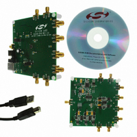
SI5356-EVB Silicon Laboratories Inc, SI5356-EVB Datasheet - Page 19

SI5356-EVB
Manufacturer Part Number
SI5356-EVB
Description
EVALUATION BOARD FOR SI5356
Manufacturer
Silicon Laboratories Inc
Specifications of SI5356-EVB
Main Purpose
Timing, Clock Generator
Utilized Ic / Part
SI5356
Technology Type
Evaluation Board
For Use With/related Products
Si5356
Lead Free Status / RoHS Status
Lead free / RoHS Compliant
Secondary Attributes
-
Embedded
-
Primary Attributes
-
Lead Free Status / Rohs Status
Lead free / RoHS Compliant
Other names
336-1750
10
12
13
14
15
16
17
18
19
11
5
6
7
8
9
SSC_DIS
VDDOD
VDDOC
VDDOB
CLK7
CLK6
CLK5
CLK4
CLK3
CLK2
INTR
OEB
VDD
SDA
SCL
VDD Core Supply Voltage.
VDD Clock Output Bank D Supply Voltage.
VDD Clock Output Bank C Supply Voltage.
VDD Clock Output Bank B Supply Voltage.
I/O
O
O
O
O
O
O
O
I
I
I
Spread Spectrum Disable.
This pin allows disabling of the spread spectrum feature on the output clocks. Connect
to 1.2 V to disable spread spectrum on all outputs. Connect to GND to enable spread
spectrum. Note that the maximum voltage level on this pin must not exceed 1.2 V. A
resistor voltage divider is recommended when controlled by a signal greater than 1.2 V.
See the Typical Application Circuit for details.
Output Enable (Active Low)
This pin allows disabling the output clocks. Connect to 1.2 V to disable all outputs.
Connect to GND to enable all outputs. Note that the maximum voltage level on this pin
must not exceed 1.2 V. A resistor voltage divider is recommended when controlled by a
signal greater than 1.2 V. See the Typical Application Circuit for details.
The device operates from a 1.8, 2.5, or 3.3 V supply. A 0.1 μF bypass capacitor should
be located very close to this pin.
Interrupt
This pin functions as an maskable interrupt output.
0 = No interrupt
1 = Interrupt present
This pin is open drain and requires an external >1 k pullup resistor.
Output Clock 7.
CMOS output clock. If unused, this pin must be left floating.
Output Clock 6.
CMOS output clock. If unused, this pin must be left floating.
Power supply for clock outputs 6 and 7. May be operated from a 1.8, 2.5, or 3.3 V sup-
ply. A 0.1 μF bypass capacitor should be located very close to this pin. If CLK6/7 are not
used, this pin must be tied to pin 7 and/or pin 24.
I
Output Clock 5.
CMOS output clock. If unused, this pin must be left floating.
Output Clock 4.
CMOS output clock. If unused, this pin must be left floating.
Power supply for clock outputs 4 and 5. May be operated from a 1.8, 2.5 or 3.3 V sup-
ply. A 0.1 μF bypass capacitor should be located very close to this pin. If CLK4/5 are not
used, this pin must be tied to pin 7 and/or pin 24.
Power supply for clock outputs 2 and 3. May be operated from a 1.8, 2.5, or 3.3 V sup-
ply. A 0.1 μF bypass capacitor should be located very close to this pin. If CLK2/3 are not
used, this pin must be tied to pin 7 and/or pin 24.
Output Clock 3.
CMOS output clock. If unused, this pin must be left floating.
Output Clock 2.
CMOS output clock. If unused, this pin must be left floating.
I
2
2
C Serial Clock Input.
C Serial Data.
Table 8. Si5356 Pin Descriptions (Continued)
Preliminary Rev. 0.3
Si5356
19


