SI5356-EVB Silicon Laboratories Inc, SI5356-EVB Datasheet - Page 13
SI5356-EVB
Manufacturer Part Number
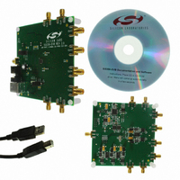
SI5356-EVB
Description
EVALUATION BOARD FOR SI5356
Manufacturer
Silicon Laboratories Inc
Specifications of SI5356-EVB
Main Purpose
Timing, Clock Generator
Utilized Ic / Part
SI5356
Technology Type
Evaluation Board
For Use With/related Products
Si5356
Lead Free Status / RoHS Status
Lead free / RoHS Compliant
Secondary Attributes
-
Embedded
-
Primary Attributes
-
Lead Free Status / Rohs Status
Lead free / RoHS Compliant
Other names
336-1750


3.7. CMOS Output Drivers
The Si5356 has 4 banks of outputs with each bank
comprised of 2 clocks for a total of 8 CMOS outputs per
device. By default, each bank of CMOS output clocks
are in-phase. Alternatively, each output clock can be
inverted. This feature enables each output pair to
operate as a differential CMOS clock. Each of the
output banks can operate from a different VDDO supply
(1.8 V, 2.5 V, 3.3 V), simplifying usage in mixed supply
applications. All clock outputs between 5 and 200 MHz
are in-phase to within ±150 ps.
The CMOS output driver has a controlled impedance in
the range of 42 to 50 which includes an internal 22
series resistor. An external series resistor is not needed
when driving 50 traces. If higher impedance traces
are used then a series resistor may be added. A typical
configuration is shown in Figure 6.
3.8. Jitter Performance
The Si5356 provides consistently low jitter for any
combination
leverages a low phase noise single PLL architecture
and Silicon Laboratories’ patented MultiSynth fractional
output divider technology to deliver period jitter less
than
configuration. This level of jitter performance is
100 ps
of
pk-pk
output
PLL
(max)
frequencies.
Figure 6. CMOS Output Driver Configuration
for
Bank C
Bank D
Bank A
Bank B
any
MultiSynth
MultiSynth
MultiSynth
MultiSynth
The
frequency
Preliminary Rev. 0.3
Si5356
device
VDDOC
VDDOD
VDDOA
CLK0
CLK1
VDDOB
CLK2
CLK3
CLK4
CLK5
CLK6
CLK7
guaranteed across process, temperature and voltage.
The Si5356 provides superior performance to traditional
multi-PLL solutions which may suffer from degraded
jitter performance depending on frequency plan and the
number of active PLLs.
3.9. Status Indicators
An interrupt pin (INTR) is available to indicate a loss of
signal (LOS) condition, a PLL loss of lock (LOL)
condition, or that the PLL is in the process of acquiring
lock (SYS_CAL). As shown in Figure 7, a status register
at address 218 is available to help identify the exact
event that caused the interrupt pin to become active. A
LOS condition occurs when there is no clock input to the
Si5356.
continuously
between the two inputs of the phase frequency detector.
When this frequency difference is greater than
1000 ppm, a loss of lock condition is declared. Note that
the VCO will track the input clock frequency for up to
~25000 ppm, which will keep the inputs to the phase
frequency detector at the same frequency until the PLL
comes out of lock. When a clock input is removed, the
interrupt pin will assert, and the clock outputs may drift
up to 5%. When the input clock is reapplied with an
appropriate frequency, the PLL will again lock.
+1.8V, +2.5V, +3.3V
+1.8V, +2.5V, +3.3V
+1.8V, +2.5V, +3.3V
+1.8V, +2.5V, +3.3V
The
monitoring
loss
of
50
50
50
50
50
50
50
50
lock
the
algorithm
frequency
Si5356
works
difference
by
13
Related parts for SI5356-EVB
Image
Part Number
Description
Manufacturer
Datasheet
Request
R

Part Number:
Description:
SMD/C°/SINGLE-ENDED OUTPUT SILICON OSCILLATOR
Manufacturer:
Silicon Laboratories Inc
Part Number:
Description:
Manufacturer:
Silicon Laboratories Inc
Datasheet:
Part Number:
Description:
N/A N/A/SI4010 AES KEYFOB DEMO WITH LCD RX
Manufacturer:
Silicon Laboratories Inc
Datasheet:
Part Number:
Description:
N/A N/A/SI4010 SIMPLIFIED KEY FOB DEMO WITH LED RX
Manufacturer:
Silicon Laboratories Inc
Datasheet:
Part Number:
Description:
N/A/-40 TO 85 OC/EZLINK MODULE; F930/4432 HIGH BAND (REV E/B1)
Manufacturer:
Silicon Laboratories Inc
Part Number:
Description:
EZLink Module; F930/4432 Low Band (rev e/B1)
Manufacturer:
Silicon Laboratories Inc
Part Number:
Description:
I°/4460 10 DBM RADIO TEST CARD 434 MHZ
Manufacturer:
Silicon Laboratories Inc
Part Number:
Description:
I°/4461 14 DBM RADIO TEST CARD 868 MHZ
Manufacturer:
Silicon Laboratories Inc
Part Number:
Description:
I°/4463 20 DBM RFSWITCH RADIO TEST CARD 460 MHZ
Manufacturer:
Silicon Laboratories Inc
Part Number:
Description:
I°/4463 20 DBM RADIO TEST CARD 868 MHZ
Manufacturer:
Silicon Laboratories Inc
Part Number:
Description:
I°/4463 27 DBM RADIO TEST CARD 868 MHZ
Manufacturer:
Silicon Laboratories Inc
Part Number:
Description:
I°/4463 SKYWORKS 30 DBM RADIO TEST CARD 915 MHZ
Manufacturer:
Silicon Laboratories Inc
Part Number:
Description:
N/A N/A/-40 TO 85 OC/4463 RFMD 30 DBM RADIO TEST CARD 915 MHZ
Manufacturer:
Silicon Laboratories Inc
Part Number:
Description:
I°/4463 20 DBM RADIO TEST CARD 169 MHZ
Manufacturer:
Silicon Laboratories Inc