SI5356-EVB Silicon Laboratories Inc, SI5356-EVB Datasheet - Page 12
SI5356-EVB
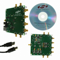
Manufacturer Part Number
SI5356-EVB
Description
EVALUATION BOARD FOR SI5356
Manufacturer
Silicon Laboratories Inc
Specifications of SI5356-EVB
Main Purpose
Timing, Clock Generator
Utilized Ic / Part
SI5356
Technology Type
Evaluation Board
For Use With/related Products
Si5356
Lead Free Status / RoHS Status
Lead free / RoHS Compliant
Secondary Attributes
-
Embedded
-
Primary Attributes
-
Lead Free Status / Rohs Status
Lead free / RoHS Compliant
Other names
336-1750


Si5356
When creating a custom RAM configuration, use the
following procedure:
1. Create a device configuration (register map) using
2. Save the configuration using the Options > Save
At this point, the new configuration can be written to the
device RAM according to the instructions in “3.5.3.
Writing a Custom Configuration to RAM”.
3.5.3. Writing a Custom Configuration to RAM
Writing a new configuration (register map) to the RAM
consists of pausing the LOL state-machine, writing new
values to the IC accounting for the write-allowed mask
given in AN565, validating the input clock or crystal,
locking the PLL to the input with the new configuration,
restarting the LOL state-machine, and calibrating the
VCO for robust operation across temperature. The flow
chart in Figure 5 on page 12 enumerates the details:
Note: The write-allowed mask specifies which bits must be
12
ClockBuilder Desktop (v2.7 or later; see "3.1.1.
ClockBuilder™ Desktop Software" on page 9) or
manually using the equations in “AN565: Configuring
the Si5356A”.
Register Map File or Options > Save C code Header
File, or create the register contents by the
conversions listed in AN565.
a. Configure the frequency plan.
b. Configure the output driver format and supply
c. Configure initial phase offset (if desired).
d. Configure spread spectrum (if desired).
read and modified before writing the entire register
byte (a.k.a. read-modify-write). “AN428: Jump Start: In-
System, Flash-Based Programming for Silicon Labs’
Timing Products” illustrates the procedure defined in
Section 3.5.2 with ANSI C code.
voltage.
U s e C lo ck B u ild e r
D e sk to p v 3 .0 o r la te r
R e g iste r
M a p
Figure 5. I
2
Preliminary Rev. 0.3
C Programming Procedure
(S e e A N 5 6 5 : C o n fig u rin g th e S i5 3 5 6 A )
a c co u n tin g fo r th e w rite -a llo w e d m a sk
W rite n e w c o n fig u ra tio n to d e vic e
S e t S O F T _ R E S E T = 1 ; re g 2 4 6 [1 ]
S e t O E B _ A L L = 1 ; re g 2 3 0 [4 ]
S e t O E B _ A L L = 0 ; re g 2 3 0 [4 ]
3.5.4. Modifying a MultiSynth Output Divider Ratio/
Any of the four output frequencies of a previously
configured Si5356 may be modified without disturbing
the other outputs. In this case, do not write the feedback
Multisynth registers. Instead, only write the set of
registers associated with the output MultiSynth divider
of interest (see “AN565: Configuring the Si5356A”).
To avoid intermediate frequencies, it is recommended
that the output to be modified is disabled before
changing the divider ratios (see AN565 for a description
of Register 230).
Any output Multisynth that is reconfigured will lose its
output
SOFT_RESET can be used to realign the outputs;
however, a soft reset will temporarily disable all outputs
in the process of realignment.
3.5.5. Writing a Custom Configuration to NVM
An alternative to ordering an Si5356 with a custom NVM
configuration is to use the field programming kit
(Si5338/56-PROG-EVB) to write directly to the NVM of
a "blank" Si5356. Since NVM is an OTP memory, it can
only be written once. The default configuration can be
reconfigured by writing to RAM through the I
(see “3.5.2. Creating a New Configuration for RAM”).
3.6. Output Phase Adjustment
The Si5356 has a digitally-controlled phase adjustment
feature that allows the user to adjust the phase of each
output clock in relation to the other output clocks. The
phase of each output clock can be adjusted with an
error of <20 ps over a range of ±45 ns. This feature is
available on any clock output that does not have Spread
Spectrum enabled.
S e t re g 2 4 1 = 0 x 6 5
A p p ly S o ft R e s e t
D isa b le O u tp u ts
E n a b le O u tp u ts
Frequency Configuration
skew
alignment
with
the
other
2
C interface
outputs.
Related parts for SI5356-EVB
Image
Part Number
Description
Manufacturer
Datasheet
Request
R

Part Number:
Description:
SMD/C°/SINGLE-ENDED OUTPUT SILICON OSCILLATOR
Manufacturer:
Silicon Laboratories Inc
Part Number:
Description:
Manufacturer:
Silicon Laboratories Inc
Datasheet:
Part Number:
Description:
N/A N/A/SI4010 AES KEYFOB DEMO WITH LCD RX
Manufacturer:
Silicon Laboratories Inc
Datasheet:
Part Number:
Description:
N/A N/A/SI4010 SIMPLIFIED KEY FOB DEMO WITH LED RX
Manufacturer:
Silicon Laboratories Inc
Datasheet:
Part Number:
Description:
N/A/-40 TO 85 OC/EZLINK MODULE; F930/4432 HIGH BAND (REV E/B1)
Manufacturer:
Silicon Laboratories Inc
Part Number:
Description:
EZLink Module; F930/4432 Low Band (rev e/B1)
Manufacturer:
Silicon Laboratories Inc
Part Number:
Description:
I°/4460 10 DBM RADIO TEST CARD 434 MHZ
Manufacturer:
Silicon Laboratories Inc
Part Number:
Description:
I°/4461 14 DBM RADIO TEST CARD 868 MHZ
Manufacturer:
Silicon Laboratories Inc
Part Number:
Description:
I°/4463 20 DBM RFSWITCH RADIO TEST CARD 460 MHZ
Manufacturer:
Silicon Laboratories Inc
Part Number:
Description:
I°/4463 20 DBM RADIO TEST CARD 868 MHZ
Manufacturer:
Silicon Laboratories Inc
Part Number:
Description:
I°/4463 27 DBM RADIO TEST CARD 868 MHZ
Manufacturer:
Silicon Laboratories Inc
Part Number:
Description:
I°/4463 SKYWORKS 30 DBM RADIO TEST CARD 915 MHZ
Manufacturer:
Silicon Laboratories Inc
Part Number:
Description:
N/A N/A/-40 TO 85 OC/4463 RFMD 30 DBM RADIO TEST CARD 915 MHZ
Manufacturer:
Silicon Laboratories Inc
Part Number:
Description:
I°/4463 20 DBM RADIO TEST CARD 169 MHZ
Manufacturer:
Silicon Laboratories Inc