AC164112 Microchip Technology, AC164112 Datasheet - Page 294
AC164112
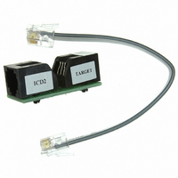
Manufacturer Part Number
AC164112
Description
VOLTAGE LIMITER MPLAB ICD2 VPP
Manufacturer
Microchip Technology
Datasheet
1.AC164112.pdf
(302 pages)
Specifications of AC164112
Accessory Type
Voltage Limiter
Product
Cable Assemblies
Features
Programming And Debugging The Latest PIC12/PIC16/PIC18 Products
Development Tool Type
Hardware - Eval/Demo Board
Lead Free Status / RoHS Status
Lead free / RoHS Compliant
For Use With/related Products
MPLAB®
Lead Free Status / Rohs Status
Lead free / RoHS Compliant
For Use With
MPLAB ICD 2
Lead Free Status / RoHS Status
Lead free / RoHS Compliant, Lead free / RoHS Compliant
Available stocks
Company
Part Number
Manufacturer
Quantity
Price
Company:

Part Number:
AC164112
Manufacturer:
Microchip Technology
Quantity:
135


PIC16F72X/PIC16LF72X
Capture Module. See Capture/Compare/PWM (CCP)
Capture/Compare/PWM (CCP)......................................... 135
CCP. See Capture/Compare/PWM (CCP)
CCP1CON Register ............................................................ 24
CCP2CON Register ............................................................ 24
CCPR1H Register ............................................................... 24
CCPR1L Register................................................................ 24
CCPR2H Register ............................................................... 24
CCPR2L Register................................................................ 24
CCPxCON Register .......................................................... 136
CKE bit ...................................................................... 175, 187
CKP bit ...................................................................... 174, 186
Clock Sources
Code Examples
Comparators
Compare Module. See Capture/Compare/PWM (CCP)
CONFIG1 Register........................................................ 95, 96
CPSCON0 Register .......................................................... 133
CPSCON1 Register .......................................................... 134
Customer Change Notification Service ............................. 299
DS41341E-page 294
Associated registers w/ Capture ............................... 138
Associated registers w/ Compare ............................. 140
Associated registers w/ PWM ................................... 144
Capture Mode ........................................................... 137
CCPx Pin Configuration ............................................ 137
Compare Mode ......................................................... 139
Interaction of Two CCP Modules (table) ................... 135
Prescaler ................................................................... 137
PWM Mode ............................................................... 141
PWM Period .............................................................. 142
Setup for PWM Operation ......................................... 143
Timer Resources....................................................... 135
External Modes ........................................................... 93
A/D Conversion ......................................................... 103
Call of a Subroutine in Page 1 from Page 0................ 30
Changing Between Capture Prescalers .................... 137
Indirect Addressing ..................................................... 31
Initializing PORTA ....................................................... 54
Initializing PORTB ....................................................... 62
Initializing PORTC....................................................... 73
Initializing PORTD....................................................... 80
Initializing PORTE ....................................................... 84
Loading the SSPBUF (SSPSR) Register .................. 170
Saving W, STATUS and PCLATH Registers
C2OUT as T1 Gate ................................................... 118
CCPx Pin Configuration .................................... 139
Software Interrupt Mode ........................... 137, 139
Special Event Trigger........................................ 139
Timer1 Mode Selection ............................. 137, 139
Duty Cycle......................................................... 142
Effects of Reset................................................. 143
Example PWM Frequencies and
Example PWM Frequencies and
Operation in Sleep Mode .................................. 143
Setup for Operation........................................... 143
System Clock Frequency Changes................... 143
EC ....................................................................... 93
HS ....................................................................... 93
LP........................................................................ 93
OST..................................................................... 93
RC....................................................................... 94
XT ....................................................................... 93
in RAM ................................................................ 45
Resolutions, 20 MHZ ................................ 143
Resolutions, 8 MHz................................... 143
Customer Notification Service .......................................... 299
Customer Support............................................................. 299
D
D/A bit ............................................................................... 187
Data Memory ...................................................................... 20
Data/Address bit (D/A)...................................................... 187
DC and AC Characteristics............................................... 241
DC Characteristics
Development Support ....................................................... 207
Device Configuration .......................................................... 95
Device Overview................................................................. 13
E
Effects of Reset
Electrical Specifications .................................................... 211
Enhanced Capture/Compare/PWM (ECCP)
Errata .................................................................................. 12
F
Firmware Instructions ....................................................... 197
Fixed Voltage Reference. See FVR
FSR Register ................................................................ 24, 25
Fuses. See Configuration Bits
FVR................................................................................... 109
FVRCON Register ...................................................... 25, 109
G
General Purpose Register File ........................................... 20
I
I
INDF Register ............................................................... 24, 25
Indirect Addressing, INDF and FSR Registers ................... 31
Instruction Format............................................................. 197
Instruction Set................................................................... 197
2
C Mode
Extended and Industrial ............................................ 218
Industrial and Extended ............................................ 212
Code Protection .......................................................... 97
Configuration Word..................................................... 95
User ID ....................................................................... 97
PWM mode ............................................................... 143
Specifications ........................................................... 230
Associated Registers ................................................ 188
ADDLW..................................................................... 199
ADDWF..................................................................... 199
ANDLW..................................................................... 199
ANDWF..................................................................... 199
MOVF ....................................................................... 202
BCF .......................................................................... 199
BSF........................................................................... 199
BTFSC ...................................................................... 199
BTFSS ...................................................................... 200
CALL......................................................................... 200
CLRF ........................................................................ 200
CLRW ....................................................................... 200
CLRWDT .................................................................. 200
COMF ....................................................................... 200
DECF ........................................................................ 200
DECFSZ ................................................................... 201
GOTO ....................................................................... 201
INCF ......................................................................... 201
INCFSZ..................................................................... 201
IORLW ...................................................................... 201
IORWF...................................................................... 201
MOVLW .................................................................... 202
© 2009 Microchip Technology Inc.
Related parts for AC164112
Image
Part Number
Description
Manufacturer
Datasheet
Request
R

Part Number:
Description:
Manufacturer:
Microchip Technology Inc.
Datasheet:
Part Number:
Description:
Manufacturer:
Microchip Technology Inc.
Datasheet:
Part Number:
Description:
Manufacturer:
Microchip Technology Inc.
Datasheet:
Part Number:
Description:
Manufacturer:
Microchip Technology Inc.
Datasheet:
Part Number:
Description:
Manufacturer:
Microchip Technology Inc.
Datasheet:
Part Number:
Description:
Manufacturer:
Microchip Technology Inc.
Datasheet:
Part Number:
Description:
Manufacturer:
Microchip Technology Inc.
Datasheet:
Part Number:
Description:
Manufacturer:
Microchip Technology Inc.
Datasheet: