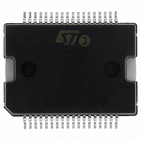
L6701 STMicroelectronics, L6701 Datasheet - Page 5

L6701
Manufacturer Part Number
L6701
Description
IC CTRLR 3PH VR10/9/K8 PWRSO-36
Manufacturer
STMicroelectronics
Datasheet
1.L6701TR.pdf
(44 pages)
Specifications of L6701
Applications
Controller, Intel VR9, VR10, K8
Voltage - Input
12V
Number Of Outputs
3
Voltage - Output
0.8 ~ 1.85 V
Operating Temperature
0°C ~ 70°C
Mounting Type
Surface Mount
Package / Case
36-PowerSOIC
Output Voltage
0.8 V to 1.85 V
Output Current
1.5 A
Switching Frequency
110 KHz
Mounting Style
SMD/SMT
Maximum Operating Temperature
+ 125 C
Minimum Operating Temperature
0 C
Lead Free Status / RoHS Status
Lead free / RoHS Compliant
Available stocks
Company
Part Number
Manufacturer
Quantity
Price
L6701
2
Figure 1.
2.1
Table 1.
Pin n
1
2
3
4
5
6
7
8
9
Pins description and connection diagrams
Pin description
°
Pins connection (Top view)
Pins description
UGATE1
PHASE1
LGATE1
LGATE2
LGATE3
BOOT1
SGND
PGND
Name
VCC
OSC / EN / FAULT
SSEND / PGOOD
All the internal references are referred to this pin. Connect to the PCB Signal
Ground.
Device Power Supply and LS driver supply.
Operative voltage is 12V ±15%. Filter with at least 1µF MLCC vs. ground.
Channel 1 LS Driver Output.
A small series resistor helps in reducing device-dissipated power.
LS Drivers return path. Connect to Power ground Plane.
Channel 2 LS Driver Output.
A small series resistor helps in reducing device-dissipated power.
Channel 3 LS Driver Output.
A small series resistor helps in reducing device-dissipated power.
Channel 1 HS driver supply.
Connect through a capacitor (100nF typ.) to PHASE1 and provide necessary
Bootstrap diode.
A small series resistor upstream the boot diode helps in reducing Boot capacitor
overcharge.
Channel 1 HS driver output.
A small series resistors helps in reducing device-dissipated power.
Channel 1 HS driver return path.
It must be connected to the HS1 MOSFET source and provides return path for
the HS driver of channel 1.
DAC_SEL
UGATE1
PHASE1
UGATE2
PHASE2
UGATE3
PHASE3
LGATE1
LGATE2
LGATE3
BOOT1
BOOT2
BOOT3
SGND
PGND
VCC
10
11
12
13
14
15
16
17
18
1
2
3
4
5
6
7
8
9
Function
36
35
34
33
32
31
30
29
28
27
26
25
24
23
22
21
20
19
2 Pins description and connection diagrams
COMP
FB
VSEN
CS-
CS+
ISEN1
ISEN2
ISEN3
FBG
FBR
VID5
VID0
VID1
VID2
VID3
VID4
REF_OUT
REF_IN
5/44


