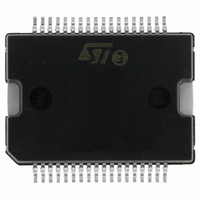
L6701 STMicroelectronics, L6701 Datasheet - Page 22

L6701
Manufacturer Part Number
L6701
Description
IC CTRLR 3PH VR10/9/K8 PWRSO-36
Manufacturer
STMicroelectronics
Datasheet
1.L6701TR.pdf
(44 pages)
Specifications of L6701
Applications
Controller, Intel VR9, VR10, K8
Voltage - Input
12V
Number Of Outputs
3
Voltage - Output
0.8 ~ 1.85 V
Operating Temperature
0°C ~ 70°C
Mounting Type
Surface Mount
Package / Case
36-PowerSOIC
Output Voltage
0.8 V to 1.85 V
Output Current
1.5 A
Switching Frequency
110 KHz
Mounting Style
SMD/SMT
Maximum Operating Temperature
+ 125 C
Minimum Operating Temperature
0 C
Lead Free Status / RoHS Status
Lead free / RoHS Compliant
Available stocks
Company
Part Number
Manufacturer
Quantity
Price
10 Output Voltage Positioning
Caution:
10.2
22/44
The device forces I
R
then given by (Offset disabled):
Where R
The whole power supply can be then represented by a "real" voltage generator with an
equivalent output resistance R
R
where R
Droop function is optional, in case it is not desired, the Current Sense circuit can be modified so
that the device always read a null current (See
CS+ directly to the output voltage leaving CS- unconnected. The reaction will keep CS+ and
CS- at the same voltage, always reading a null current and also assuring the FB disconnection
protection to be effective.
Figure 8.
Fully-Differential Load-Line (Droop Function - Optional)
Fully-Differential current-reading for voltage-positioning allows the designer to save time in the
application fine-tuning since the BOM so obtained becomes layout-independent. The patent-
pending topology offered by L6701 allow implementing fully-differential current-sense still using
only two current-sense pins (CS+ and CS-).
used to implement the Fully-Differential Droop-Function. The current flowing across the three
inductors is read through an R
each phase to program the trans-conductance-gain. As previously mentioned, a current I
proportional to the average of the currents of the three phases is internally generated, mirrored
PHASE1
PHASE2
PHASE3
FB
FB
implementing the load regulation dependence. The output characteristic vs. load current is
resistor can be then designed according to the R
D
V
LL
O UT
is typically designed to have I
CS+
is the resulting load-line resistance implemented by the system.
Droop Function Current Reading Network
C
L1
L2
L3
Droop Function Enabled
PH
=
VID R
DROOP
R
DCR1
DCR2
DCR3
D
CS-
–
I
CS
------------ -
DCR
FB
x 3
= I
V
OUT
I
L
DROOP
CS
⋅
I
PH
LL
DROOP
x3, proportional to the read current, into the feedback resistor
=
FB
and a voltage value of VID.
- C
R
F
R
-------------------------- -
R
FB
PH
PH
R
C
F
=
3
⋅
FB
filter for each phase as well as an R
CS
C
COMP
VID R
PH
= 35µA at the maximum output current (OCP).
=
Figure 9
R
=>
–
Figure
L L
PHASE1
PHASE2
PHASE3
FB
I
⋅
CS
------------ -
DCR
R
⋅
LL
shows the typical Current-Sense Circuit
DCR
------------ - I
D
=
8). To do this, it is enough to connect
R
specifications as follow:
D
I
------------
O UT
3
CS+
⋅
OUT
⋅
DCR
------------ -
Droop Function Disabled
L1
L2
L3
R
D
=
DCR1
DCR2
DCR3
VID R
CS-
I
CS
–
x 3
V
D
OUT
I
DROOP
LL
is required for
⋅
I
FB
O UT
R
F
R
FB
C
F
L6701
CS
COMP


