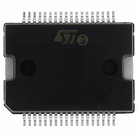
L6701 STMicroelectronics, L6701 Datasheet - Page 40

L6701
Manufacturer Part Number
L6701
Description
IC CTRLR 3PH VR10/9/K8 PWRSO-36
Manufacturer
STMicroelectronics
Datasheet
1.L6701TR.pdf
(44 pages)
Specifications of L6701
Applications
Controller, Intel VR9, VR10, K8
Voltage - Input
12V
Number Of Outputs
3
Voltage - Output
0.8 ~ 1.85 V
Operating Temperature
0°C ~ 70°C
Mounting Type
Surface Mount
Package / Case
36-PowerSOIC
Output Voltage
0.8 V to 1.85 V
Output Current
1.5 A
Switching Frequency
110 KHz
Mounting Style
SMD/SMT
Maximum Operating Temperature
+ 125 C
Minimum Operating Temperature
0 C
Lead Free Status / RoHS Status
Lead free / RoHS Compliant
Available stocks
Company
Part Number
Manufacturer
Quantity
Price
16 Layout Guidelines
16.3
40/44
Embedding L6701-based VRs
When embedding the VR into the application, additional care must be taken since the whole VR
is a switching DC/DC regulator and the most common systems in which it has to work are
digital systems such as MB or similar. In fact, latest MB has become faster and powerful: high
speed data bus are more and more common and switching-induced noise produced by the VR’
MOSFETs can affect data integrity if not following additional layout guidelines. Few easy points
must be considered mainly when routing traces and planes in which high switching currents
flow (high switching currents cause voltage spikes across the stray inductance of the trace
causing noise that can affect the near traces):
Keep safe guarding distance between high current switching VRD traces and data buses,
especially if high-speed data bus to minimize noise coupling.
Keep safe guard distance or filter properly when routing bias traces for I/O sub-systems that
must walk near the VRD.
Possible causes of noise can be located in the PHASE connections, MOSFET gate drive and
Input voltage path (from input bulk capacitors and HS drain). Also PGND connections must be
considered if not insisting on a power ground plane. These connections must be carefully kept
far away from noise-sensitive data bus.
Since the generated noise is mainly due to the switching activity of the VR, noise emissions
depend on how fast the current switches. To reduce noise emission levels, it is also possible, in
addition to the previous guidelines, to reduce the current slope by properly tuning the HS gate
resistor and the PHASE snubber network.
L6701


