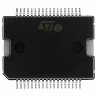
L6701 STMicroelectronics, L6701 Datasheet - Page 31

L6701
Manufacturer Part Number
L6701
Description
IC CTRLR 3PH VR10/9/K8 PWRSO-36
Manufacturer
STMicroelectronics
Datasheet
1.L6701TR.pdf
(44 pages)
Specifications of L6701
Applications
Controller, Intel VR9, VR10, K8
Voltage - Input
12V
Number Of Outputs
3
Voltage - Output
0.8 ~ 1.85 V
Operating Temperature
0°C ~ 70°C
Mounting Type
Surface Mount
Package / Case
36-PowerSOIC
Output Voltage
0.8 V to 1.85 V
Output Current
1.5 A
Switching Frequency
110 KHz
Mounting Style
SMD/SMT
Maximum Operating Temperature
+ 125 C
Minimum Operating Temperature
0 C
Lead Free Status / RoHS Status
Lead free / RoHS Compliant
Available stocks
Company
Part Number
Manufacturer
Quantity
Price
L6701
13.5
13.6
Figure 14. Feedback Disconnection
PGOOD (Only for VR9 and K8 Modes)
It is an open-drain signal set free after the soft-start sequence has finished. It is pulled low
when the output voltage drops below -230mV of the programmed voltage.
Over Current Protection
Output current in each phase is monitored by L6701 through R
value of these resistors, it is possible to set the OCP to the desired value. The Over Current
threshold has to be programmed to a safe value, in order to be sure that the device doesn't
enter OCP during normal operation of the device. This value must take into consideration also
the extra current needed during the Dynamic VID Transition I
across MOSFETs R
elements. Moreover, since also the internal threshold spreads, the Rg design has to consider
the minimum value I
where I
Quasi-Constant-Current.
Since the device reads the current across Low Side MOSFETs, it limits the bottom of the
inductor current entering in constant current until setting UVP as below explained. I
be calculated starting from the corresponding output current value I
must also be considered when D-VID are supported) since the device holds the valley current
information:
where I
Current, I
required by D-VID (when applicable). In particular, since the device limits the valley of the
PHASE1
PHASE2
PHASE3
OCPx
OUT(OCP)
PP
is the inductor current ripple in each phase and I
is the current measured by the current reading circuitry when the device enters
R
D
R
CS_DROOP+
is still the output current value at which the device enters Quasi-Constant-
D
R
D
DS(on)
OCTH(min)
L1
L2
L3
C
D
, the process spread and temperature variations of these sensing
R
DCR1
DCR2
DCR3
G
I
O CPx
of the threshold as follow:
CS_DROOP-
I
Rg
INFO
x 3
V
=
OUT
=
I
DROOP
I
----------------------------------------------------------------- -
I
--------------------------- -
OCPx m ax
OUT O CP
VID
FB
3
(
R
F
(
R
I
O CTH m in
FB
C
)
)
F
FB_DISCONNECTED
–
⋅
R
1V
∆I
----------- -
(
COMP
dsO N max
2
PP
)
13 Output voltage Monitor and Protections
+
(
I
------------------
VSEN
D VID
D-VID
D-VID
–
3
)
ISEN
FBR
is the additional current
and, since the device reads
OUT(OCP)
and so, programming the
FBG
as follow (I
OCPx
D-VID
must
31/44


