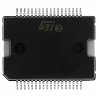
L6701 STMicroelectronics, L6701 Datasheet - Page 29

L6701
Manufacturer Part Number
L6701
Description
IC CTRLR 3PH VR10/9/K8 PWRSO-36
Manufacturer
STMicroelectronics
Datasheet
1.L6701TR.pdf
(44 pages)
Specifications of L6701
Applications
Controller, Intel VR9, VR10, K8
Voltage - Input
12V
Number Of Outputs
3
Voltage - Output
0.8 ~ 1.85 V
Operating Temperature
0°C ~ 70°C
Mounting Type
Surface Mount
Package / Case
36-PowerSOIC
Output Voltage
0.8 V to 1.85 V
Output Current
1.5 A
Switching Frequency
110 KHz
Mounting Style
SMD/SMT
Maximum Operating Temperature
+ 125 C
Minimum Operating Temperature
0 C
Lead Free Status / RoHS Status
Lead free / RoHS Compliant
Available stocks
Company
Part Number
Manufacturer
Quantity
Price
L6701
13
13.1
13.2
Output voltage Monitor and Protections
L6701 monitors through pin VSEN the regulated voltage in order to manage the OVP, UVP and
PGOOD (when applicable) conditions. Protections are active also during soft-start (See
Section 12
cycle delay after the transition has finished to avoid false triggering.
In addition, preliminary over-voltage protection is also provided to protect the load from high-
side MOSFET failures before the system turn-ON.
Under Voltage
If the output voltage monitored by VSEN drops more than -400mV below the programmed
reference for more than one clock period, the device turns off all MOSFETs driving high the
FAULT pin and latches the condition: to recover it is required to cycle Vcc or the EN pin. This is
independent by the selected operative mode.
Preliminary Over Voltage
To provide a protection while VCC is below the UVLO
damage to the load in case of failed HS MOSFETs. In fact, since the device is supplied from the
12V bus, it is basically “blind” for any voltage below the turn-on threshold (UVLO
to give full protection to the load, a preliminary-OVP protection is provided while VCC is within
UVLO
According to the DAC_SEL pin status, this protection turns-on the low side MOSFETs as long
as the FBR pin voltage is greater than 1.9V for VR10 and 2.1V for VR9 and K8 with a 300mV
hysteresis (See
source voltage depending on the voltage applied to VCC. This protection depends also on the
EN pin status as detailed in
all operative modes with intervention thresholds dependent on the DAC_SEL pin status.
A simple way to provide protection to the output in all conditions when the system is OFF (then
avoiding the unprotected red region in
through the 5VSB bus with an OR-ing diode solution as shown in
always present before +12V and, in case of HS short, the LS MOSFET is driven with 5V
assuring a reliable protection of the load.
When using the OR-ing diode solution, OR-ing diodes need to be sized according to the device
current consumption: the two diodes will then results to be different since the diode connected
to the 12V bus needs to carry the current for normal operations (I
to the 5V
active. Device current consumption (I
MOSFET configuration as follow:
Device current consumption when Pre-OVP is active depends on the output filter configuration
since LS MOSFETs switching frequency depends on the leakage that is charging the output
filter. Test on the bench is required but, for an over-sized solution, the same diode identified for
the +12V bus can be used.
VCC
SB
and UVLO
for details) while are masked during D-VID transitions with an additional 32 clock
(I
RMS-PREOVP
I
RMS
Table
=
OVP
10). When set, the protection drives the LS MOSFET with a gate-to-
3 F
⋅
.
) need to carry only the current in case of Pre-OVP protection is
SW
Figure
⋅
(
Q
G HS
13. Preliminary OVP is always active before UVLO
RMS
Figure
+
Q
) in normal operations depends on the external
GLS
13-Left) consists in supplying the controller
)
+
(
I
CC
VCC
+
13 Output voltage Monitor and Protections
3 I
threshold is fundamental to avoid
⋅
CCDRx
RMS
Figure
+
) and the diode connected
3 I
⋅
13-Right: 5VSB is
BOO Tx
)
VCC
). In order
VCC
29/44
for


