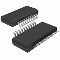
LTC1644CGN#TR Linear Technology, LTC1644CGN#TR Datasheet - Page 9

LTC1644CGN#TR
Manufacturer Part Number
LTC1644CGN#TR
Description
IC CONTROLLER HOT SWAP 20-SSOP
Manufacturer
Linear Technology
Type
Hot-Swap Controllerr
Datasheet
1.LTC1644CGNPBF.pdf
(24 pages)
Specifications of LTC1644CGN#TR
Applications
CompactPCI™
Internal Switch(s)
No
Voltage - Supply
3.3V, 5V, ±12V
Operating Temperature
0°C ~ 70°C
Mounting Type
Surface Mount
Package / Case
20-SSOP (0.154", 3.91mm Width)
Family Name
LTC1644
Package Type
SSOP N
Operating Supply Voltage (min)
2.75/10.8/-10.8V
Operating Supply Voltage (max)
13.2/-14V
Operating Temperature (min)
0C
Operating Temperature (max)
70C
Operating Temperature Classification
Commercial
Product Depth (mm)
3.99mm
Product Height (mm)
1.5mm
Mounting
Surface Mount
Pin Count
20
Lead Free Status / RoHS Status
Contains lead / RoHS non-compliant
Lead Free Status / RoHS Status
Contains lead / RoHS non-compliant
Other names
LTC1644CGNTR
Available stocks
Company
Part Number
Manufacturer
Quantity
Price
PI FU CTIO S
OFF/ON (Pin 5): Digital Input. Connect the CPCI BD_SEL#
signal to the OFF/ON pin. When the OFF/ON pin is pulled
low, the GATE pin is pulled high by a 65 A current source
and the internal 12V and –12V switches are turned on.
When the OFF/ON pin is pulled high, the GATE pin will be
pulled to ground by a 225 A current source and the 12V
and –12V switches turn off.
The OFF/ON pin is also used to reset the electronic circuit
breaker. If the OFF/ON pin is cycled high and low following
the trip of the circuit breaker, the circuit breaker is reset
and a normal power-up sequence will occur.
FAULT (Pin 6): Open-Drain Digital I/O. FAULT is pulled low
when a current limit fault is detected. Current limit faults
are ignored until the voltage at the TIMER pin is within 1V
of 12V
pull low and the chip latches off in the event of an
overcurrent fault. The chip will remain latched in the off
state until the OFF/ON pin is cycled high then low.
Forcing the FAULT pin low with an external pull-down will
cause the chip to be latched into the off state after a 45 s
deglitching time.
PWRGD (Pin 7): Open-Drain Digital Power Good Output.
Connect the CPCI HEALTHY# signal to the PWRGD pin.
PWRGD remains low while V
2.9V, V
the supplies falls below its power good threshold voltage,
PWRGD will go high after a 10 s deglitching time.
GND (Pin 8): Chip Ground.
RESETIN (Pin 9): Digital Input. Connect the CPCI PCI_RST#
signal to the RESETIN pin. Pulling RESETIN low will cause
RESETOUT to pull low.
RESETOUT (Pin 10): Open-Drain Digital Output. Connect
the CPCI LOCAL_PCI_RST# signal to the RESETOUT pin.
RESETOUT is the logical combination of RESETIN and
PWRGD.
DRIVE (Pin 11): Precharge Base Drive Output. Provides
base drive for an external NPN emitter-follower which in
turn biases the PRECHARGE node.
PRECHARGE (Pin 12): Precharge Monitor Input. An on-
chip error amplifier servos the DRIVE pin voltage to keep
the precharge node at 1V.
U
IN
5VOUT
. Once the TIMER cycle is complete, FAULT will
U
4.62V and V
U
EEOUT
12VOUT
–10.5V. When any of
11.1V, V
3VOUT
5V
lockout circuit prevents the switches from turning on
when the voltage at the 5V
5V input supply is available, tie the 5V
5V
resistor placed in the supply path between 5V
5V
a constant 51mV across the sense resistor and a constant
current through the switch while the TIMER pin is low. A
foldback feature reduces the current limit as the voltage at
the 5V
When the TIMER pin is high, the circuit breaker function is
enabled. If the voltage across the sense resistor exceeds
55mV but is less than 150mV, the circuit breaker is tripped
after a 45 s time delay. In the event the sense resistor
voltage exceeds 150mV, the circuit breaker trips immedi-
ately and the chip latches off. To disable the current limit,
5V
GATE (Pin 15): High Side Gate Drive for the External 3.3V
and 5V N-Channels pass transistors. Requires an external
series RC network to compensate the current limit loop
and set the minimum ramp-up rate. During power up, the
slope of the voltage rise at the GATE is set by the 65 A
current source connected to 12V
pacitor connected to GND (C1, see Figure 1) or by the 3.3V
or 5V current limit and the bulk capacitance on the 3V
or 5V
Figure 1). During power down, the slew rate of the GATE
voltage is set by the 225 A current source connected to
GND and the external GATE capacitor (C1, see Figure 1).
The voltage at the GATE pin will be modulated to maintain
a constant current when either the 3V or 5V supplies go
into current limit while the TIMER pin is low. In the event
of a fault or an undervoltage condition, the GATE pin is
immediately pulled to GND.
3V
resistor placed in the supply path between 3V
3V
a constant 51mV across the sense resistor and a constant
current through the switch while the TIMER pin is low. A
foldback feature reduces the current limit as the voltage at
the 3V
IN
SENSE
SENSE
SENSE
SENSE
SENSE
(Pin 13): 5V Supply Sense Input. An undervoltage
OUT
OUT
OUT
, the GATE pin voltage will be adjusted to maintain
, the GATE pin voltage will be adjusted to maintain
(Pin 14): 5V Current Limit Sense. With a sense
and 5V
(Pin 16): 3.3V Current Limit Set. With a sense
supply lines (C
pin approaches GND.
pin approaches GND.
IN
can be shorted together.
LOAD(5VOUT)
IN
pin is less than 2.48V. If no
IN
and the external ca-
or C
IN
LTC1644
LOAD(3VOUT)
to the 3V
IN
IN
IN
, see
pin.
9
and
and
OUT
1644f


