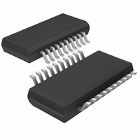
LTC1644CGN#TR Linear Technology, LTC1644CGN#TR Datasheet - Page 21

LTC1644CGN#TR
Manufacturer Part Number
LTC1644CGN#TR
Description
IC CONTROLLER HOT SWAP 20-SSOP
Manufacturer
Linear Technology
Type
Hot-Swap Controllerr
Datasheet
1.LTC1644CGNPBF.pdf
(24 pages)
Specifications of LTC1644CGN#TR
Applications
CompactPCI™
Internal Switch(s)
No
Voltage - Supply
3.3V, 5V, ±12V
Operating Temperature
0°C ~ 70°C
Mounting Type
Surface Mount
Package / Case
20-SSOP (0.154", 3.91mm Width)
Family Name
LTC1644
Package Type
SSOP N
Operating Supply Voltage (min)
2.75/10.8/-10.8V
Operating Supply Voltage (max)
13.2/-14V
Operating Temperature (min)
0C
Operating Temperature (max)
70C
Operating Temperature Classification
Commercial
Product Depth (mm)
3.99mm
Product Height (mm)
1.5mm
Mounting
Surface Mount
Pin Count
20
Lead Free Status / RoHS Status
Contains lead / RoHS non-compliant
Lead Free Status / RoHS Status
Contains lead / RoHS non-compliant
Other names
LTC1644CGNTR
Available stocks
Company
Part Number
Manufacturer
Quantity
Price
APPLICATIO S I FOR ATIO
sinusoidal response whose duration and period is depen-
dent on the resonant circuit parameters. Since the abso-
lute maximum supply voltage of the LTC1644 is 13.2V,
transient protection against 12V
age spikes and ringing is highly recommended.
In these applications, there are two methods for eliminat-
ing these supply voltage transients: using Zener diodes to
clip the transient to a safe level and snubber networks.
Snubber networks are series RC networks whose time
constants are experimentally determined based on the
board’s parasitic resonant circuits. As a starting point, the
capacitors in these networks are chosen to be 10 to 100
the power MOSFET’s C
is a value determined experimentally and ranges from 1
to 50 , depending on the parasitic resonant circuit. Note
Z1
Figure 16. Place Transient Protection Devices
Close to LTC1644’s 12V
Z1, Z2: SMAJ12CA
*ADDITIONAL DETAILS OMITTED FOR CLARITY
0.01 F
C4
R15
1
U
12V
12V
Figure 15. Place Transient Protection Devices Close to LTC1644’s 5V
OSS
LTC1644*
IN
1
IN
GND
5V
3V
3.3V
Z3, Z4: 1PMT5.0AT3
*ADDITIONAL DETAILS OMITTED FOR CLARITY
IN
U
Z3
8
under bias. The series resistor
5V
–12V
IN
IN
V
and V
EEIN
IN
2
IN
EEIN
and V
W
3V
Pins
R16
1
IN
17
C5
0.01 F
0.005
R1
1644 F16
EEIN
3V
SENSE
supply volt-
Z2
16
U
IRF7413
GATE
Q1
15
R3
10
Figure 17. Recommended Layout for Transient Protection Components
3V
LTC1644*
OUT
GND PLANE
18
GND
VIAS TO
8
5V
that in all LTC1644 circuit schematics, zener diodes and
snubber networks have been added to the 12V
(–12V) supply rail and should be used always. Since the
absolute maximum supply voltage of the LTC1644 is
13.2V, snubber networks are not necessary on the 3V
the 5V
mended as these devices provide large-scale transient
protection for the LTC1644 against PCI backplane fault
occurrences. All protection networks should be mounted
very close to the LTC1644’s supply voltage using short
lead lengths to minimize lead inductance. This is shown
schematically in Figures 15 and 16 and a recommended
layout of the transient protection devices around the
LTC1644 is shown in Figure 17.
IN
0.007
13
R2
R14
R13
C5
C4
5V
IN
*ADDITIONAL DETAILS OMITTED FOR CLARITY
DRAWING IS NOT TO SCALE!
SENSE
supply lines. Zener diodes, however, are recom-
14
IRF7413
Q2
Z3
Z1
Z2
12V
R4
10
5V
IN
OUT
3
R5
1k
IN
V
1644 F15
5V
5V
3V
3.3V
and 3V
EEIN
0.047 F
OUT
OUT
C1
3V
Z4
IN
IN
LTC1644*
Pins
5V
GND
LTC1644
IN
IN
and V
1644 F17
21
Z4
IN
EEIN
1644f
or


