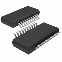
LTC1644CGN#TR Linear Technology, LTC1644CGN#TR Datasheet - Page 18

LTC1644CGN#TR
Manufacturer Part Number
LTC1644CGN#TR
Description
IC CONTROLLER HOT SWAP 20-SSOP
Manufacturer
Linear Technology
Type
Hot-Swap Controllerr
Datasheet
1.LTC1644CGNPBF.pdf
(24 pages)
Specifications of LTC1644CGN#TR
Applications
CompactPCI™
Internal Switch(s)
No
Voltage - Supply
3.3V, 5V, ±12V
Operating Temperature
0°C ~ 70°C
Mounting Type
Surface Mount
Package / Case
20-SSOP (0.154", 3.91mm Width)
Family Name
LTC1644
Package Type
SSOP N
Operating Supply Voltage (min)
2.75/10.8/-10.8V
Operating Supply Voltage (max)
13.2/-14V
Operating Temperature (min)
0C
Operating Temperature (max)
70C
Operating Temperature Classification
Commercial
Product Depth (mm)
3.99mm
Product Height (mm)
1.5mm
Mounting
Surface Mount
Pin Count
20
Lead Free Status / RoHS Status
Contains lead / RoHS non-compliant
Lead Free Status / RoHS Status
Contains lead / RoHS non-compliant
Other names
LTC1644CGNTR
Available stocks
Company
Part Number
Manufacturer
Quantity
Price
APPLICATIO S I FOR ATIO
LTC1644
(3) the gate-source (V
R
on four parameters: current delivered to the load, I
device R
ambient,
which the circuit will be exposed, T
parameters determine the junction temperature of the
MOSFET. For reliable circuit operation, the maximum
junction temperature (T
not exceed the manufacturer’s recommended value. For a
given set of conditions, the junction temperature of a
power MOSFET is given by Equation 9:
18
I/O PIN 128
DS(ON)
BD_SEL#
LONG 5V
GROUND
I/O PIN 1
Figure 8. Precharge Voltage <1V Application Circuit
5V
. Power MOSFET power dissipation is dependent
DS(ON)
CONNECTOR
BACKPLANE
JA
Z4: 1PMT5.0AT3
*ADDITIONAL PINS OMITTED FOR CLARITY
GND
V
*ADDITIONAL DETAILS OMITTED FOR CLARITY
; and the maximum ambient temperature to
PRECHARGE
8
C3 4.7nF
PRECHARGE OUT
; device thermal resistance, junction-to-
R10A
U
CONNECTOR
BACKPLANE
=
PCB EDGE
R10A + R10B
LTC1644*
R10B
18
GS
J(MAX)
R9
PRECHARGE DRIVE
R10A
) voltage drive for the specified
U
12
DATA BUS
) for a power MOSFET should
• 1V
R22 2.74
MMBT2222A
C7
0.01 F
A(MAX)
11
C9 0.1 F
PER 10
POWER PINS
W
Z4
12
Figure 10. Precharge Circuit with Bus Switch
R8
R7
1k
. All four of these
5V
1644 F08
3V
IN
51k 5%
IN
R23
U
R20
1.2k
5%
Q2
MMBT3906
1k 5%
LOAD
R24
75k
5%
R19
13
5
;
5V
OFF/ON
10 5%
10 5%
IN
R13
R14
where P
PCB layout techniques for optimal thermal management
of power MOSFET power dissipation help to keep device
section for more information.
The R
to make its drain-source voltage (V
of 3V
0.1V yields a 3% error at maximum load current. This
JA
MOSFET Junction Temperature,
T
GND
J(MAX)
as low as possible. See PCB Layout Considerations
IN
DS(ON)
Figure 9. Precharge Voltage >1V Application Circuit
8
18 5%
or 5V
R10
D
PRECHARGE
= I
GND
V
*ADDITIONAL DETAILS OMITTED FOR CLARITY
LOAD
of the external pass transistor should be low
T
IN
OE
PRECHARGE
12
A(MAX)
8
. For example, at 3V
R10A
PRECHARGE
BUS SWITCH
• R
LTC1644*
R11
10k
5%
=
DS(ON)
+
12
LTC1644*
C3 4.7nF
R10A + R10B
PRECHARGE OUT
R10B
C3 4.7nF
R10A
JA
R12
10k
5%
• P
UP TO 128 I/O LINES
18
D
R9
• 1V
24
MMBT2222A
R9
DRIVE
PRECHARGE OUT
I
MMBT2222A
OUT
11
DS
IN
1V 10%
DRIVE
= 55mA
) a small percentage
Q1
= 3.3V, V
11
12
R8
R7
1k
3V
1644 F09
IN
12 5%
1k 5%
I/O
I/O
R7
R8
DS
+ V
BRIDGE
CHIP
PCI
CB
3V
1644 F10
1644f
(9)
IN
=


