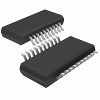
LTC1644CGN#TR Linear Technology, LTC1644CGN#TR Datasheet - Page 20

LTC1644CGN#TR
Manufacturer Part Number
LTC1644CGN#TR
Description
IC CONTROLLER HOT SWAP 20-SSOP
Manufacturer
Linear Technology
Type
Hot-Swap Controllerr
Datasheet
1.LTC1644CGNPBF.pdf
(24 pages)
Specifications of LTC1644CGN#TR
Applications
CompactPCI™
Internal Switch(s)
No
Voltage - Supply
3.3V, 5V, ±12V
Operating Temperature
0°C ~ 70°C
Mounting Type
Surface Mount
Package / Case
20-SSOP (0.154", 3.91mm Width)
Family Name
LTC1644
Package Type
SSOP N
Operating Supply Voltage (min)
2.75/10.8/-10.8V
Operating Supply Voltage (max)
13.2/-14V
Operating Temperature (min)
0C
Operating Temperature (max)
70C
Operating Temperature Classification
Commercial
Product Depth (mm)
3.99mm
Product Height (mm)
1.5mm
Mounting
Surface Mount
Pin Count
20
Lead Free Status / RoHS Status
Contains lead / RoHS non-compliant
Lead Free Status / RoHS Status
Contains lead / RoHS non-compliant
Other names
LTC1644CGNTR
Available stocks
Company
Part Number
Manufacturer
Quantity
Price
APPLICATIO S I FOR ATIO
LTC1644
restricts the choice of power MOSFETs to those devices
with very low R
that can be used with the LTC1644.
Power MOSFETs are classified into two categories: stan-
dard MOSFETs (R
level MOSFETs (R
external pass transistors are required for the 3.3V and 5V
supply rails, logic-level power MOSFETs should be used
with the LTC1644.
Overvoltage Transient Protection
Good engineering practice calls for bypassing the supply
rail of any analog circuit. Bypass capacitors are often
placed at the supply connection of every active device, in
addition to one or more large-value bulk bypass capacitors
per supply rail. If power is connected abruptly, the large
bypass capacitors slow the rate of rise of the supply
voltage and heavily damp any parasitic resonance of lead
20
LONG 5V
GROUND
5V
DS(ON)
CONNECTOR
BACKPLANE
D1, D2: BAV99
Z4: 1PMT5.0AT3
*ADDITIONAL PINS OMITTED FOR CLARITY
DS(ON)
DS(ON)
U
. Table 9 lists some power MOSFETs
specified at V
CONNECTOR
BACKPLANE
U
specified at V
PCB EDGE
BD_SEL#
GROUND
W
R22 2.74
GS
C6
0.01 F
CONNECTOR
BACKPLANE
*ADDITIONAL PINS OMITTED FOR CLARITY
Figure 14. BD_SEL# Pushbutton Toggle Switch
Figure 13. No 3.3V Supply Application Circuit
= 10V) and logic-
GS
C9 0.1 F
PER 10
POWER PINS
Z4
= 5V). Since
5V
8
U
CONNECTOR
IN
BACKPLANE
GND
PCB EDGE
3V
IN
17
D1
D2
NC
3V
PUSHBUTTON
SENSE
16
SWITICH
or PC track inductance working against the supply bypass
capacitors.
The opposite is true for LTC1644 Hot Swap circuits
mounted on plug-in cards. In most cases, there is no
supply bypass capacitor present on the powered 12V
(12V
3.3V (3V
abrupt connection, produced by inserting the board into a
backplane connector, results in a fast rising edge applied
on these input supply lines of the LTC1644.
Since there is no bulk capacitance to damp the parasitic
track inductance, supply voltage transients excite para-
sitic resonant circuits formed by the power MOSFET
capacitance and the combined parasitic inductance from
the wiring harness, the backplane and the circuit board
traces. These ringing transients appear as a fast edge on
the input supply lines, exhibiting a peak overshoot up to
2.5 times the steady-state value followed by a damped
100
5V
IN
IN
13
), –12V (V
0.007
R2
IN
5V
) or the 5V (5V
LTC1644*
5V
IN
1.2k
SENSE
14
1k
EEIN
5
8
IRF7413
GATE
OFF/ON
GND
Q2
LTC1644*
) of the PCB edge connector or on the
15
R4
10
IN
1644 F14
) side of the MOSFET switch. An
5V
OUT
3
3V
OUT
18
R5
1k
1644 F13
0.047 F
C1
5V
OUT
1644f


