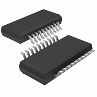
LTC1644CGN#TR Linear Technology, LTC1644CGN#TR Datasheet - Page 13

LTC1644CGN#TR
Manufacturer Part Number
LTC1644CGN#TR
Description
IC CONTROLLER HOT SWAP 20-SSOP
Manufacturer
Linear Technology
Type
Hot-Swap Controllerr
Datasheet
1.LTC1644CGNPBF.pdf
(24 pages)
Specifications of LTC1644CGN#TR
Applications
CompactPCI™
Internal Switch(s)
No
Voltage - Supply
3.3V, 5V, ±12V
Operating Temperature
0°C ~ 70°C
Mounting Type
Surface Mount
Package / Case
20-SSOP (0.154", 3.91mm Width)
Family Name
LTC1644
Package Type
SSOP N
Operating Supply Voltage (min)
2.75/10.8/-10.8V
Operating Supply Voltage (max)
13.2/-14V
Operating Temperature (min)
0C
Operating Temperature (max)
70C
Operating Temperature Classification
Commercial
Product Depth (mm)
3.99mm
Product Height (mm)
1.5mm
Mounting
Surface Mount
Pin Count
20
Lead Free Status / RoHS Status
Contains lead / RoHS non-compliant
Lead Free Status / RoHS Status
Contains lead / RoHS non-compliant
Other names
LTC1644CGNTR
Available stocks
Company
Part Number
Manufacturer
Quantity
Price
APPLICATIO S I FOR ATIO
LOCAL_PCI_RST#
TIMER
During a power-up sequence, a 21 A current source is
connected to the TIMER pin (Pin 4) and current limit faults
are ignored until the voltage ramps to within 1V of 12V
(Pin 1). This feature allows the chip to power up CPCI
boards with widely varying capacitive loads on the sup-
plies. The power-up time for any one of the four outputs is
given by Equation 2:
where XV
For example, for C
7A and I
t
ON
PRECHARGE
HEALTHY#
BD_SEL#
XV
10V/DIV
10V/DIV
10V/DIV
10V/DIV
10V/DIV
12V
V
5V/DIV
5V/DIV
5V/DIV
5V/DIV
5V/DIV
TIMER
5V
3V
EEOUT
GATE
OUT
OUT
OUT
OUT
LOAD(5VOUT)
OUT
Figure 2. Normal Power-Up Sequence
= 5V
2
OUT
LOAD(5VOUT)
U
I
LIMIT XVOUT
= 5A, the 5V
, 3V
C
LOAD XVOUT
(
U
OUT
, 12V
(
10ms/DIV
= 2000 F, I
)
OUT
OUT
W
I
)
LOAD XVOUT
turn-on time will be
or V
XV
(
OUT
EEOUT
LIMIT(5VOUT)
U
)
(–12V).
1644 F02
(2)
IN
=
LOCAL_PCI_RST#
~10ms. By substituting the variables in Equation 2 with the
appropriate values, the turn-on time for the other three
outputs can be calculated.
The timer period should be set longer than the maximum
supply turn-on time but short enough to not exceed the
maximum safe operating area of the pass transistor during
a short circuit. The timer period for the LTC1644 is given
by:
As a design aid, the timer period as a function of the timing
capacitor using standard values from 0.01 F to 1 F is
shown in Table 2.
PRECHARGE
t
HEALTHY#
TIMER
BD_SEL#
10V/DIV
10V/DIV
10V/DIV
10V/DIV
10V/DIV
12V
V
5V/DIV
5V/DIV
5V/DIV
5V/DIV
5V/DIV
TIMER
5V
3V
EEOUT
GATE
OUT
OUT
OUT
Figure 3. Normal Power-Down Sequence
C
TIMER
21
A
11
V
10ms/DIV
LTC1644
13
1644f
(3)
1644 F03


