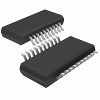
LTC1644CGN#TR Linear Technology, LTC1644CGN#TR Datasheet - Page 12

LTC1644CGN#TR
Manufacturer Part Number
LTC1644CGN#TR
Description
IC CONTROLLER HOT SWAP 20-SSOP
Manufacturer
Linear Technology
Type
Hot-Swap Controllerr
Datasheet
1.LTC1644CGNPBF.pdf
(24 pages)
Specifications of LTC1644CGN#TR
Applications
CompactPCI™
Internal Switch(s)
No
Voltage - Supply
3.3V, 5V, ±12V
Operating Temperature
0°C ~ 70°C
Mounting Type
Surface Mount
Package / Case
20-SSOP (0.154", 3.91mm Width)
Family Name
LTC1644
Package Type
SSOP N
Operating Supply Voltage (min)
2.75/10.8/-10.8V
Operating Supply Voltage (max)
13.2/-14V
Operating Temperature (min)
0C
Operating Temperature (max)
70C
Operating Temperature Classification
Commercial
Product Depth (mm)
3.99mm
Product Height (mm)
1.5mm
Mounting
Surface Mount
Pin Count
20
Lead Free Status / RoHS Status
Contains lead / RoHS non-compliant
Lead Free Status / RoHS Status
Contains lead / RoHS non-compliant
Other names
LTC1644CGNTR
Available stocks
Company
Part Number
Manufacturer
Quantity
Price
APPLICATIO S I FOR ATIO
LTC1644
Power-Up Sequence
The LTC1644 is specifically designed for live insertion and
removal of CPCI boards. The typical application is shown
in Figure 1. The 3.3V, 5V, 12V and –12V inputs to the
LTC1644 come from the medium length power pins. The
long 5V and 3.3V connector pins are connected through
decoupling resistors to the medium length 5V and 3.3V
connector pins on the CPCI plug-in card and provide early
power for the LTC1644’s precharge circuit, pull-up resis-
tors and the PCI bridge chip. The BD_SEL# signal is
connected to the OFF/ON pin while the PWRGD pin is
connected to the HEALTHY# signal. The HEALTHY# signal
is combined with the PCI_RST# signal on-chip to generate
the LOCAL_PCI_RST# signal which is available at the
RESETOUT pin.
The power supplies are controlled by placing external
N-channel pass transistors in the 3.3V and 5V power paths
and internal pass transistors for the 12V and –12V power
paths (Figure 1).
Resistors R1 and R2 provide current fault detection and
R5 and C1 provide current control loop compensation.
Resistors R3 and R4 prevent high frequency oscillations
in Q1 and Q2. Shunt RC snubbers R15-C4 and R16-C5 and
zener diodes Z1 and Z2 prevent the 12V
respectively, from ringing beyond the absolute maximum
rated supply voltages during hot insertion.
When the CPCI card is inserted, the long 5V and 3.3V
connector pins and GND pins make contact first. The
LTC1644’s precharge circuit biases the bus I/O pins to 1V
during this stage of the insertion (Figure 2). The 12V, –12V
and 5V and 3.3V medium length pins make contact during
the next stage of insertion. At this point the LTC1644
powers on but slot power is disabled as long as the OFF/ON
pin is pulled high by the 1.2k pull-up resistor to 5V
During the final stage of board insertion, the BD_SEL#
short connector pin makes contact and the OFF/ON pin can
12
U
U
W
IN
and V
U
EEIN
pins,
IN
.
be pulled low. This enables the pass transistors to turn on
and a 21 A current source is connected to TIMER (Pin 4).
The current in each pass transistor increases until it
reaches the current limit for each supply. The 5V and 3.3V
supplies are then allowed to power up based on one of the
following rates:
Power-up rate:
whichever is slower.
Current limit faults are ignored while the TIMER pin
voltage is ramping up and is less than 1V below 12V
1). Once all four supply voltages are within tolerance,
HEALTHY# (Pin 7) will pull low and LOCAL_PCI_RST# is
free to follow PCI_RST#.
Power-Down Sequence
When the BD_SEL# is pulled high, a power-down
sequence begins (Figure 3).
Internal switches are connected to each of the output
supply voltage pins to discharge the bypass capacitors to
ground. The TIMER pin is immediately pulled low. The
GATE pin (Pin 15) is pulled down by a 225 A current
source to prevent the load currents on the 3.3V and 5V
supplies from going to zero instantaneously and glitching
the power supply voltages. When any of the output volt-
ages dips below its threshold, the HEALTHY# signal pulls
high and LOCAL_PCI_RST# will be asserted low.
Once the power-down sequence is complete, the CPCI
card may be removed from the slot. During extraction, the
precharge circuit will continue to bias the bus I/O pins at
1V until the 5V and 3.3V long connector pin connections
are broken.
dV
dt
65
C
1
A
,
or
C
LOAD VOUT
I
LIMIT V
(
5
(
5
)
)
,
or
C
LOAD VOUT
I
LIMIT V
(
3
(
3
IN
(Pin
)
1644f
(1)
)


