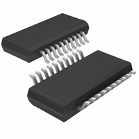
LTC1644CGN#TR Linear Technology, LTC1644CGN#TR Datasheet - Page 17

LTC1644CGN#TR
Manufacturer Part Number
LTC1644CGN#TR
Description
IC CONTROLLER HOT SWAP 20-SSOP
Manufacturer
Linear Technology
Type
Hot-Swap Controllerr
Datasheet
1.LTC1644CGNPBF.pdf
(24 pages)
Specifications of LTC1644CGN#TR
Applications
CompactPCI™
Internal Switch(s)
No
Voltage - Supply
3.3V, 5V, ±12V
Operating Temperature
0°C ~ 70°C
Mounting Type
Surface Mount
Package / Case
20-SSOP (0.154", 3.91mm Width)
Family Name
LTC1644
Package Type
SSOP N
Operating Supply Voltage (min)
2.75/10.8/-10.8V
Operating Supply Voltage (max)
13.2/-14V
Operating Temperature (min)
0C
Operating Temperature (max)
70C
Operating Temperature Classification
Commercial
Product Depth (mm)
3.99mm
Product Height (mm)
1.5mm
Mounting
Surface Mount
Pin Count
20
Lead Free Status / RoHS Status
Contains lead / RoHS non-compliant
Lead Free Status / RoHS Status
Contains lead / RoHS non-compliant
Other names
LTC1644CGNTR
Available stocks
Company
Part Number
Manufacturer
Quantity
Price
APPLICATIO S I FOR ATIO
Output Voltage Monitor
The status of all four output voltages is monitored by the
power good function. In addition, the PCI_RST# signal is
logically combined on-chip with the HEALTHY# signal to
create LOCAL_PCI_RST# (see Table 5). As a result,
LOCAL_PCI_RST# will be pulled low whenever HEALTHY#
is pulled high independent of the state of the PCI_RST#
signal.
Table 5. LOCAL_PCI_RST# Truth Table
If any of the output voltages drop below the power good
threshold for more than 10 s, the PWRGD pin will be
pulled high and the LOCAL_PCI_RST# signal will be
asserted low.
Precharge
The PRECHARGE input and DRIVE output pins are in-
tended for use in generating the 1V precharge voltage that
is used to bias the bus I/O connector pins during board
insertion. The LTC1644 is also capable of generating
precharge voltages other than 1V. Figure 8 shows a circuit
that can be used in applications requiring a precharge
voltage less than 1V. The circuit in Figure 9 can be used for
applications that need precharge voltages greater than 1V.
Table 6 lists suggested resistor values for R10A and R10B
vs precharge voltage for the application circuits shown in
Figures 8 and 9.
Table 6. R10A and R10B Resistor Values vs Precharge Voltage
Due to leakage current constraints, precharge resistor
values of less than 50k are often required. In these
V
PCI_RST#
PRECHARGE
1.5V
1.4V
1.3V
1.2V
1.1V
1V
LO
LO
HI
HI
R10A
18
18
18
18
18
18
U
HEALTHY#
9.09
7.15
5.36
3.65
1.78
R10B
LO
LO
HI
HI
0
U
V
PRECHARGE
0.9V
0.8V
0.7V
0.6V
0.5V
W
LOCAL_PCI_RST#
16.2
14.7
12.1
9.09
R10A
11
LO
LO
LO
HI
U
1.78
3.65
5.11
7.15
9.09
R10B
precharge applications, it may also be necessary to dis-
connect the individual resistors from the LTC1644’s
PRECHARGE pin when the plug-in board is completely
seated in the board slot. The circuit in Figure 10 uses a bus
switch to connect the individual precharge resistors to the
LTC1644’s PRECHARGE pin while the BD_SEL# pin volt-
age is pulled up to 5V
connector pin is still unconnected. After the plug-in board
is completely seated, the BD_SEL# pin voltage will drop to
approximately 3.8V (assuming BD_SEL# isn’t asserted
low), and the bus switch OE pin is pulled high by Q2. When
the plug-in card is removed from the connector, the
BD_SEL# connection is broken first and the BD_SEL# pin
voltage pulls up to 5V. This causes Q2 to turn off, which re-
enables the bus switch and the precharge resistors are
reconnected to the LTC1644’s PRECHARGE pin for the
remainder of the board extraction process.
Other CompactPCI Applications
The LTC1644 can be easily configured for applications
where no V
V
For CPCI applications where no 5V supply input is re-
quired, short both the 5V
pin and short the 5V
If no 3.3V supply input is required, Figure 13 illustrates
how the LTC1644 should be configured. First, 3V
(Pin 16) is connected to 3V
connected to 5V
connected through a pair of signal diodes (BAV99) to 5V
For applications where the BD_SEL# connector pin is
typically grounded on the backplane, the circuit in
Figure 14 allows the LTC1644 to be reset simply by
pressing a pushbutton switch on the CPCI plugin board.
This arrangement eliminates the requirement to extract
and reinsert the CPCI board in order to reset the LTC1644’s
circuit breakers.
Power MOSFET Selection Criteria
Three device parameters are key in selecting the optimal
power MOSFET for Hot Swap applications. The three
parameters are: (1) device power dissipation (P
device drain-source channel ON resistance, R
EEIN
pin to GND and floating the V
EE
supply is present by simply connecting the
OUT
(Pin 3) and the LTC1644’s 3V
OUT
IN
pin to the 3V
, i.e., when the BD_SEL# short
IN
IN
and 5V
(Pin 17), 3V
SENSE
EEOUT
OUT
LTC1644
pins to the 3V
pin (Figure 11).
pin (Figure 12).
OUT
DS(ON)
(Pin 18) is
IN
17
D
SENSE
); (2)
pin is
; and
1644f
IN
IN
.


