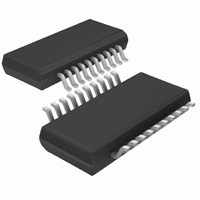
LTC1644CGN#TR Linear Technology, LTC1644CGN#TR Datasheet - Page 10

LTC1644CGN#TR
Manufacturer Part Number
LTC1644CGN#TR
Description
IC CONTROLLER HOT SWAP 20-SSOP
Manufacturer
Linear Technology
Type
Hot-Swap Controllerr
Datasheet
1.LTC1644CGNPBF.pdf
(24 pages)
Specifications of LTC1644CGN#TR
Applications
CompactPCI™
Internal Switch(s)
No
Voltage - Supply
3.3V, 5V, ±12V
Operating Temperature
0°C ~ 70°C
Mounting Type
Surface Mount
Package / Case
20-SSOP (0.154", 3.91mm Width)
Family Name
LTC1644
Package Type
SSOP N
Operating Supply Voltage (min)
2.75/10.8/-10.8V
Operating Supply Voltage (max)
13.2/-14V
Operating Temperature (min)
0C
Operating Temperature (max)
70C
Operating Temperature Classification
Commercial
Product Depth (mm)
3.99mm
Product Height (mm)
1.5mm
Mounting
Surface Mount
Pin Count
20
Lead Free Status / RoHS Status
Contains lead / RoHS non-compliant
Lead Free Status / RoHS Status
Contains lead / RoHS non-compliant
Other names
LTC1644CGNTR
Available stocks
Company
Part Number
Manufacturer
Quantity
Price
PI FU CTIO S
RESETIN 9
LTC1644
When the TIMER pin is high, the circuit breaker function is
enabled. If the voltage across the sense resistor exceeds
55mV but is less than 150mV, the circuit breaker is tripped
after a 45 s time delay. In the event the sense resistor
voltage exceeds 150mV, the circuit breaker trips immedi-
ately and the chip latches off. To disable the current limit,
3V
3V
lockout circuit prevents the switches from turning on
when the voltage at the 3V
3.3V input supply is available, connect two series diodes
between 5V
cathode of second diode to 3V
BLOCK DIAGRA
10
PWRGD 7
OFF/ON 5
FAULT 6
SENSE
IN
U
(Pin 17): 3.3V Supply Sense Input. An undervoltage
NOTE: V
Q11
Q10
5V
2.5V
UVL
13
and 3V
8.3V
UVL
IN
150mV, TIMER HI
51mV, TIMER LO
12VIN
U
IN
TIMER
55mV
+–
+–
– V
and 3V
TIMER
IN
5V
12V
< 1V = TIMER HI, V
SENSE
1
14
can be shorted together.
IN
IN
+–
+
–
U
12V
(tie anode of first diode to 5V
CP1
Q9
20
OUT
5V
–
+
OUT
W
IN
Q8
A1
12VIN
pin is less than 2.48V. If no
REF
– V
IN
TIMER
, see Figure 11).
+
–
> 1V = TIMER LOW
CP7
GATE
Q1
15
12V
TIMER
12V
IN
4
65 A
LOGIC
IN
Q7
225 A
21 A
IN
and
V
EEIN
2
A2
V
3V
output supply voltage. The PWRGD pin cannot pull low
until the 3V
supply is available, tie the 3V
V
connected between V
ceed –10.5V before the PWRGD pin pulls low unless the
V
pin.
12V
connected between 12V
exceed 11.1V before the PWRGD pin can pull low.
3V
EEOUT
Q6
19
+
EEOUT
EE
OUT
–
OUT
Q5
CP2
OUT
PWRGD function is disabled by grounding the V
–
+
+
–
(Pin 18): Analog Input used to monitor the 3.3V
16
(Pin 19): –12V Supply Output. A 1
(Pin 20): 12V Supply Output. A 0.5 switch is
150mV, TIMER HI
51mV, TIMER LO
REF
3V
OUT
SENSE
TIMER
55mV
–
–
+
+
2.5V
UVL
+
–
pin voltage exceeds 2.9V. If no 3.3V input
3V
17
CP5
IN
EEIN
GND
IN
and V
8
and 12V
CP3
CP4
DRIVE
OUT
11
Q12
EEOUT
pin to the 5V
+
–
+
–
Q2
REF
REF
Q3
3V
OUT
18
. V
OUT
A3
. 12V
5V
EEOUT
OUT
3
–
+
OUT
Q4
OUT
1V
switch is
must ex-
10
12
1644 BD
pin.
RESETOUT
PRECHARGE
must
EEIN
1644f


