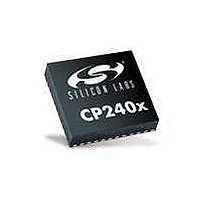
CP2401-GQ Silicon Laboratories Inc, CP2401-GQ Datasheet - Page 101

CP2401-GQ
Manufacturer Part Number
CP2401-GQ
Description
IC LCD DRIVER 48TQFP
Manufacturer
Silicon Laboratories Inc
Specifications of CP2401-GQ
Package / Case
48-TQFP, 48-VQFP
Display Type
LCD
Configuration
128 Segment
Interface
I²C, SMBus
Current - Supply
620µA
Voltage - Supply
1.8 V ~ 3.6 V
Operating Temperature
-40°C ~ 85°C
Mounting Type
Surface Mount
Data Ram Size
256 B
Interface Type
I2C, SMBus
Maximum Clock Frequency
25 MHz
Number Of Timers
2
Operating Supply Voltage
1.8 V to 3.6 V
Maximum Operating Temperature
+ 85 C
Mounting Style
SMD/SMT
Minimum Operating Temperature
- 40 C
Lead Free Status / RoHS Status
Lead free / RoHS Compliant
Digits Or Characters
-
Lead Free Status / Rohs Status
Lead free / RoHS Compliant
Other names
336-1860
Available stocks
Company
Part Number
Manufacturer
Quantity
Price
Company:
Part Number:
CP2401-GQ
Manufacturer:
Silicon Laboratories Inc
Quantity:
10 000
Part Number:
CP2401-GQ
Manufacturer:
SILICON LABS/芯科
Quantity:
20 000
Company:
Part Number:
CP2401-GQR
Manufacturer:
Silicon Laboratories Inc
Quantity:
10 000
14. Serial Peripheral Interface (SPI)
CP2400/2 devices have a 4-wire Serial Peripheral Interface which provides access to the internal registers and
memory. A typical connection to a SPI master is shown in Figure 14.1.
14.1. Signal Descriptions
The four signals used by the SPI (MOSI, MISO, SCK, NSS) are described below.
14.1.1. Master Out, Slave In (MOSI)
The master-out, slave-in (MOSI) signal is an output from a master device and an input to slave devices. It is used
to serially transfer data from the master to the slave. This signal is always in input for CP2402/1 devices. Data is
transferred most-significant bit first.
14.1.2. Master In, Slave Out (MISO)
The master-in, slave-out (MISO) signal is an output from a slave device and an input to the master device. It is
used to serially transfer data from the slave to the master. This signal is always an output for CP2402/1 devices.
Data is transferred most-significant bit first. The MISO pin is placed in a high-impedance state when the slave
select (NSS) signal is de-asserted.
14.1.3. Serial Clock (SCK)
The serial clock (SCK) signal is an output from the master device and an input to slave devices. It is used to
synchronize the transfer of data between the master and slave on the MOSI and MISO lines. This signal is always
an input for CP2402/1 devices. The SCK signal is ignored when the slave select (NSS) signal is de-asserted.
14.1.4. Slave Select (NSS)
The active-low slave-select (NSS) signal allows support for multiple slave devices on a single bus. It is also used
by the CP2402/1 to detect the start and end of a SPI transfer.
Master
Device
GPIO
Figure 14.1. SPI Connection Diagram
GPIO
GPIO
MISO
MOSI
SCK
NSS
Rev. 1.0
INT
MISO
MOSI
SCK
NSS
INT
MISO
MOSI
SCK
NSS
Device
Device
Slave
Slave
CP2400/1/2/3
101


