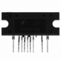
FSFA2100 Fairchild Semiconductor, FSFA2100 Datasheet - Page 11

FSFA2100
Manufacturer Part Number
FSFA2100
Description
IC SWIT OVP UVLO 9SIP
Manufacturer
Fairchild Semiconductor
Datasheet
1.FSFA2100.pdf
(16 pages)
Specifications of FSFA2100
Output Isolation
Isolated
Frequency Range
94 ~ 106kHz
Voltage - Input
14.5 ~ 25 V
Voltage - Output
650V
Power (watts)
200W
Operating Temperature
-40°C ~ 130°C
Package / Case
9-SIP
Output Voltage
25 V
Output Current
8 A
Output Power
450 W
Switching Frequency
300 KHz
Operating Temperature Range
- 40 C to + 130 C
Mounting Style
Through Hole
Duty Cycle (max)
55 %
Lead Free Status / RoHS Status
Lead free / RoHS Compliant
Available stocks
Company
Part Number
Manufacturer
Quantity
Price
© 2008 Fairchild Semiconductor Corporation
FSFA2100 • Rev. 1.0.0
3.1 Pulse-by-Pulse Current Limit: In normal operation,
the duty cycle of the low-side MOSFET is determined by
comparing the internal triangular signal with the
feedback voltage. However, the low-side MOSFET is
forced to turn off when the current sense pin voltage
reaches -0.58V. This operation limits the drain current
below a pre-determined level to avoid the destruction of
the MOSFETs.
3.2 Abnormal Over-Current Protection (AOCP): If one
of the secondary rectifier diodes is short-circuited, large
current with extremely high di/dt can flow through the
MOSFET before OCP or OLP is triggered. AOCP is
triggered with a very short shutdown delay time when the
sensed voltage drops below -0.9V. This protection is
latch mode and reset only when LV
3.3 Overload Protection (OLP): Overload is defined as
the load current exceeding its nominal level due to an
unexpected
protection circuit should trigger to protect the power
supply. However, even when the power supply is in the
normal condition, the OLP circuit can be triggered during
the load transition. To avoid this undesired operation, the
OLP circuit is designed to trigger only after a specified
time to determine whether it is a transient situation or a
true overload situation. Because of the pulse-by-pulse
current limit capability, the maximum peak current
Figure 21. Half-Wave Sensing
Figure 22. Full-Wave Sensing
abnormal
event.
In
CC
is pulled below 5V.
this
situation, a
11
through the MOSFET is limited; and, therefore, the
maximum input power is restricted with a given input
voltage. If the output consumes more than this maximum
power, the output voltage (V
nominal voltage. This reduces the current through the
opto-coupler diode, which also reduces the opto-coupler
transistor current, increasing the feedback voltage (V
If V
blocked and the OLP current source starts to charge C
slowly, as shown in Figure 23. In this condition, V
continues increasing until it reaches 7V, then the
switching operation is terminated, as shown in Figure 23.
The delay time for shutdown is the time required to
charge C
A 30 ~ 50ms delay time is typical for most applications.
3.4 Over-Voltage Protection (OVP): When the LV
reaches 23V, OVP is triggered. This protection is
enabled when using an auxiliary winding of the
transformer to supply LV
3.5 Thermal Shutdown (TSD): The MOSFETs and the
control IC are built in one package. This allows the
control IC to detect the abnormal over-temperature of the
MOSFET. If the temperature exceeds approximately
130 ° C, the thermal shutdown triggers.
4. Soft-Start: At startup, the duty cycle starts increasing
slowly to establish the correct working conditions for
transformers, inductors, and capacitors. The voltage on
the output capacitors is progressively increased to
smoothly establish the required output voltage. Soft-start
time is internally implemented for 15ms (when the
operating frequency is set to 100kHz.) In addition, to
help the soft-start operation, a capacitor and a resistor
would be connected on the R
in Figure 24. Before the power supply is powered on, the
capacitor C
C
t
SS
delay
FB
becomes charged progressively by the current
exceeds 3V, D1, which is illustrated in Figure 19, is
=
7V
3V
V
7 (
I
ds
O
B
V
from 3V to 7V with 5µA, as given by:
-
SS
5
Figure 23. Overload Protection
3
V
μ
A
)
remains fully discharged. After power-on,
×
C
t
1
B
V
CC
Overload protection
FB
to FPS.
t
delay
T
O
pin externally, as shown
) decreases below the
Vc
www.fairchildsemi.com
t
2
I
LIM
t
(2)
FB
CC
FB
).
B


