FSFA2100 Fairchild Semiconductor, FSFA2100 Datasheet
FSFA2100
Specifications of FSFA2100
Available stocks


Related parts for FSFA2100


FSFA2100 Summary of contents
Page 1
... Compared with discrete MOSFET and PWM controller solution, FSFA2100 can reduce total cost; simultaneously increasing efficiency, productivity, and system reliability. Maximum Output ...
Page 2
... Application Circuit Diagram Figure 1. Typical Application Circuit for an Asymmetric PWM Half-Bridge Converter Figure 2. Typical Application Circuit for an Asymmetric PWM Flyback Converter © 2008 Fairchild Semiconductor Corporation FSFA2100 • Rev. 1.0 LVcc HVcc R T Control CTR sense LVcc HVcc R T Control V FB ...
Page 3
... Block Diagram © 2008 Fairchild Semiconductor Corporation FSFA2100 • Rev. 1.0.0 Figure 3. Internal Block Diagram 3 www.fairchildsemi.com ...
Page 4
... This pin is the power ground. This pin is connected to the source of the low-side MOSFET This pin is the supply voltage of the control IC connection This is the supply voltage of the high-side gate-drive circuit IC This is the drain of the low-side MOSFET. Typically, a transformer is connected to this pin. CTR © 2008 Fairchild Semiconductor Corporation FSFA2100 • Rev. 1.0 LVcc HVcc FB Figure 4 ...
Page 5
... The maximum value of the recommended operating junction temperature is limited by thermal shutdown. Thermal Impedance T =25°C unless otherwise specified. A Symbol θ Junction-to-Case Center Thermal Impedance (Both MOSFETs Conducting) JC © 2008 Fairchild Semiconductor Corporation FSFA2100 • Rev. 1.0.0 =25°C unless otherwise specified. A Parameter -V and V DL CTR Pin to Low-Side Drain Voltage (3) ...
Page 6
... I Feedback Source Current FB V Burst Mode High-Threshold Voltage BH V Burst Mode Low-Threshold Voltage BL V Burst Mode Hysteresis Voltage BHY t Internal Soft-Start Time SS © 2008 Fairchild Semiconductor Corporation FSFA2100 • Rev. 1.0.0 Test Conditions I =200μ =200μ =10V =0V, I (5) GS Diode dI /dt=100A/μ ...
Page 7
... D Dead Time T Notes: 5. This parameter, although guaranteed, is not tested in production. 6. These parameters, although guaranteed, are tested only in EDS (wafer test) process. © 2008 Fairchild Semiconductor Corporation FSFA2100 • Rev. 1.0.0 (Continued) Parameter Test Conditions ΔV/Δt=-1V/µs V (5) ΔV/Δt=-1V/µs (5) Δ ...
Page 8
... Temp (℃) Figure 7. High-Side V (HV CC 1.1 1.05 1 0.95 0.9 -40 -20 0 Temp (℃) Figure 9. Low-Side V (LV CC © 2008 Fairchild Semiconductor Corporation FSFA2100 • Rev. 1.0.0 =25ºC. A 1.1 1.05 1 0.95 0 100 Figure 6. Switching Frequency vs. Temperature 1.1 1.05 1 0.95 0 100 ) Start vs. Temperature Figure 8. High-Side ...
Page 9
... Temp (℃) Figure 13. LV OVP Voltage vs. Temperature CC 1.1 1.05 1 0.95 0.9 -40 -20 0 Temp (℃) Figure 15. V Voltage vs. Temperature BH © 2008 Fairchild Semiconductor Corporation FSFA2100 • Rev. 1.0.0 (Continued) =25ºC. A 1.1 1.05 1 0.95 0 100 1.1 1.05 1 0.95 0 100 1.1 1 ...
Page 10
... The latch is reset only when LV below 5V. Figure 20. Protection blocks Low-side MOSFET current should be sensed for Pulse- by-pulse current limit and AOCP. The FSFA2100 senses drain current as a negative voltage, as shown in Figure 21 and Figure 22. Half-wave sensing allows low-power dissipation in the sensing resistor, while full-wave sensing has less noise in the sensing signal ...
Page 11
... Because of the pulse-by-pulse current limit capability, the maximum peak current © 2008 Fairchild Semiconductor Corporation FSFA2100 • Rev. 1.0.0 through the MOSFET is limited; and, therefore, the maximum input power is restricted with a given input voltage. If the output consumes more than this maximum power, the output voltage (V nominal voltage ...
Page 12
... MHz can be added on the drain-to-source terminals of each MOSFET to divide the DC link voltage. pin DL 6. Burst Operation: To minimize power dissipation in standby mode, the FSFA2100 enters burst-mode operation. As the load decreases, the feedback voltage is charged, SS decreases. As shown in Figure 25, the device automatically enters burst mode when the feedback ...
Page 13
... Features High Efficiency ( >93% at 400V Reduced EMI Noise through Zero-Voltage-Switching (ZVS) Enhanced System Reliability with Various Protection Functions Internal Soft-Start (15ms) © 2008 Fairchild Semiconductor Corporation FSFA2100 • Rev. 1.0.0 Input Voltage Range Rated Output Power 400V input) IN Figure 26. Typical Application Circuit ...
Page 14
... Bobbin: EER3542 (Horizontal) EER3542 Pin(S → → → → Inductance Leakage © 2008 Fairchild Semiconductor Corporation FSFA2100 • Rev. 1.0.0 (Continued Figure 27. Core and Winding Wire 0.12φ×30 (Litz wire) 0.1φ×100 (Litz wire) 0.1φ×100 (Litz wire) ...
Page 15
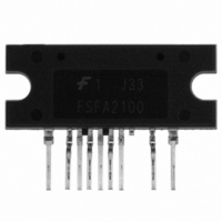
... Package specifications do not expand the terms of Fairchild’s worldwide terms and conditions, specifically the warranty therein, which covers Fairchild products. Always visit Fairchild Semiconductor’s online packaging area for the most recent package drawings: http://www.fairchildsemi.com/packaging/. © 2008 Fairchild Semiconductor Corporation FSFA2100 • Rev. 1.0.0 Figure 28. 9-SIP Package 15 www.fairchildsemi.com ...
Page 16
... Fairchild Semiconductor Corporation FSFA2100 • Rev. 1.0.0 16 www.fairchildsemi.com ...