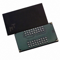
MT48H4M16LFB4-8 IT Micron Technology Inc, MT48H4M16LFB4-8 IT Datasheet - Page 15

MT48H4M16LFB4-8 IT
Manufacturer Part Number
MT48H4M16LFB4-8 IT
Description
IC SDRAM 64MBIT 125MHZ 54VFBGA
Manufacturer
Micron Technology Inc
Datasheet
1.MT48H4M16LFB4-10.pdf
(54 pages)
Specifications of MT48H4M16LFB4-8 IT
Format - Memory
RAM
Memory Type
Mobile SDRAM
Memory Size
64M (4M x 16)
Speed
125MHz
Interface
Parallel
Voltage - Supply
1.7 V ~ 1.9 V
Operating Temperature
-40°C ~ 85°C
Package / Case
54-VFBGA
Lead Free Status / RoHS Status
Lead free / RoHS Compliant
Operation
Bank/row Activation
issued to a bank within the SDRAM, a row in that bank
must be “opened.” This is accomplished via the
ACTIVE command, which selects both the bank and
the row to be activated (see Figure 7, Activating a Spe-
cific Row in a Specific Bank Register).
a READ or WRITE command may be issued to that row,
subject to the
be divided by the clock period and rounded up to the
next whole number to determine the earliest clock
edge after the ACTIVE command on which a READ or
WRITE command can be entered. For example, a
specification of 20ns with a 125 MHz clock (8ns
period) results in 2.5 clocks, rounded to 3. This is
reflected in Figure 8, which covers any case where 2 <
t
convert other specification limits from time units to
clock cycles.)
in the same bank can only be issued after the previous
active row has been “closed” (precharged). The mini-
mum time interval between successive ACTIVE com-
mands to the same bank is defined by
can be issued while the first bank is being accessed,
which results in a reduction of total row-access over-
pdf: 09005aef80a63953, source: 09005aef808a7edc
Y25L_64Mb_2.fm - Rev. E 11/04 EN
RCD (MIN)/
Before any READ or WRITE commands can be
After opening a row (issuing an ACTIVE command),
A subsequent ACTIVE command to a different row
A subsequent ACTIVE command to another bank
t
CK
t
RCD specification.
Figure 8: Meeting
3. (The same procedure is used to
COMMAND
CLK
t
RCD (MIN) should
ACTIVE
T0
t
RC.
t
RCD (MIN) when 2 <
t
NOP
T1
RCD
t
RCD
15
head. The minimum time interval between successive
ACTIVE commands to different banks is defined by
t
Figure 7: Activating a Specific Row in a
RRD.
A0–A10, A11
T2
NOP
Micron Technology, Inc., reserves the right to change products or specifications without notice.
BA0, BA1
RAS#
CAS#
WE#
CKE
CLK
CS#
Specific Bank Register
t
RCD (MIN)/
READ or
WRITE
T3
HIGH
DON’T CARE
MOBILE SDRAM
t
©2003 Micron Technology, Inc. All rights reserved.
T4
CK< 3
ADDRESS
ADDRESS
BANK
ROW
64Mb: x16
DON’T CARE


