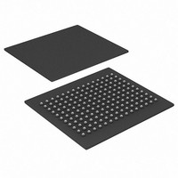
CY7C1460AV25-200BZC Cypress Semiconductor Corp, CY7C1460AV25-200BZC Datasheet - Page 17

CY7C1460AV25-200BZC
Manufacturer Part Number
CY7C1460AV25-200BZC
Description
IC SRAM 36MBIT 200MHZ 165LFBGA
Manufacturer
Cypress Semiconductor Corp
Datasheet
1.CY7C1460AV25-200BZC.pdf
(27 pages)
Specifications of CY7C1460AV25-200BZC
Format - Memory
RAM
Memory Type
SRAM - Synchronous
Memory Size
36M (1M x 36)
Speed
200MHz
Interface
Parallel
Voltage - Supply
2.375 V ~ 2.625 V
Operating Temperature
0°C ~ 70°C
Package / Case
165-LFBGA
Lead Free Status / RoHS Status
Contains lead / RoHS non-compliant
Available stocks
Company
Part Number
Manufacturer
Quantity
Price
Company:
Part Number:
CY7C1460AV25-200BZC
Manufacturer:
Cypress Semiconductor Corp
Quantity:
10 000
Document #: 38-05354 Rev. *D
Maximum Ratings
(Above which the useful life may be impaired. For user guide-
lines, not tested.)
Storage Temperature ................................. –65°C to +150°C
Ambient Temperature with
Power Applied............................................. –55°C to +125°C
Supply Voltage on V
Supply Voltage on V
DC to Outputs in Tri-State ................... –0.5V to V
DC Input Voltage....................................–0.5V to V
Electrical Characteristics
DC Electrical Characteristics
V
V
V
V
V
V
I
I
I
I
I
I
I
Notes:
14. Overshoot: V
15. T
X
OZ
DD
SB1
SB2
SB3
SB4
Parameter
DD
DDQ
OH
OL
IH
IL
Power-up
: Assumes a linear ramp from 0V to V
IH
Power Supply Voltage
I/O Supply Voltage
Output HIGH Voltage
Output LOW Voltage
Input HIGH Voltage
Input LOW Voltage
Input Leakage Current
except ZZ and MODE
Input Current of MODE Input = V
Input Current of ZZ
Output Leakage Current GND ≤ V
V
Automatic CE
Power-down
Current—TTL Inputs
Automatic CE
Power-down
Current—CMOS Inputs
Automatic CE
Power-down
Current—CMOS Inputs
Automatic CE
Power-down
Current—TTL Inputs
(AC) < V
DD
Operating Supply
DD
DDQ
Description
DD
Relative to GND........ –0.5V to +3.6V
+1.5V (Pulse width less than t
Relative to GND ...... –0.5V to +V
Over the Operating Range
Over the Operating Range
[14]
[14]
DD
for 2.5V I/O
for 1.8V I/O
for 2.5V I/O, I
for 1.8V I/O, I
for 2.5V I/O, I
for 1.8V I/O, I
for 2.5V I/O
for 1.8V I/O
for 2.5V I/O
for 1.8V I/O
GND ≤ V
Input = V
Input = V
Input = V
V
f = f
Max. V
V
1/t
Max. V
V
f = 0
Max. V
V
f = f
Max. V
V
DD
IN
IN
IN
IN
(min.) within 200 ms. During this time V
CYC
MAX
MAX
≥ V
≤ 0.3V or V
≤ 0.3V or V
≥ V
= Max., I
DD
DD
DD
DD
IH
IH
CYC
= 1/t
= 1/t
DDQ
I
SS
DD
SS
DD
I
, Device Deselected,
, Device Deselected,
, Device Deselected,
, Device Deselected,
or V
or V
≤ V
≤ V
/2), undershoot: V
DD
CYC
CYC
OUT
OH
OH
OL
OL
DDQ
DDQ,
+ 0.5V
+ 0.5V
IN
IN
IN
IN
≤ V
= 1.0 mA
= 100 µA,
≤ V
= −1.0 mA
= –100 µA
> V
> V
DD
= 0 mA,
Test Conditions
Output Disabled
IL
IL
[14, 15]
DDQ
DDQ
, f = f
, f = 0
IL
− 0.3V,
− 0.3V,
Current into Outputs (LOW)......................................... 20 mA
Static Discharge Voltage.......................................... > 2001V
(per MIL-STD-883, Method 3015)
Latch-up Current.................................................... > 200 mA
Operating Range
(AC)> –2V (Pulse width less than t
Commercial
Industrial
MAX
Range
=
IH
4-ns cycle, 250 MHz
5-ns cycle, 200 MHz
6-ns cycle, 167 MHz
All speed grades
All speed grades
All speed grades
All speed grades
< V
DD
–40°C to +85°C
and V
Temperature
0°C to +70°C
Ambient
DDQ
< V
DD
CYC
.
/2).
2.5V –5%/+5% 1.7V to V
2.375
2.375
Min.
1.26
–0.3
–0.3
–30
1.7
2.0
1.6
1.7
–5
–5
–5
CY7C1460AV25
CY7C1462AV25
CY7C1464AV25
V
DD
V
V
DD
DD
2.625
Max.
V
0.36
435
385
335
185
120
160
135
Page 17 of 27
1.9
0.4
0.2
0.7
30
+ 0.3V
+ 0.3V
5
5
5
DD
V
DDQ
Unit
mA
mA
mA
mA
mA
mA
mA
µA
µA
µA
µA
µA
µA
V
V
V
V
V
V
V
V
V
V
V
DD
[+] Feedback


